System and method for selectivity etching an integrated circuit

a selectivity etching and integrated circuit technology, applied in semiconductor/solid-state device testing/measurement, semiconductor device details, semiconductor/solid-state device testing/measurement, etc., can solve the problem of process saving considerable time, achieve enhanced chemical etching process, reduce the use of fib tools, and save considerable time

Inactive Publication Date: 2008-07-22
QUALCOMM INC
View PDF7 Cites 2 Cited by
  • Summary
  • Abstract
  • Description
  • Claims
  • Application Information

AI Technical Summary

Benefits of technology

[0012]The present invention describes an improved method to minimize the use of FIB tools in accessing a desired IC die region through a bulk Si wafer. A thin layer of polyimide, or other suitable material, is deposited on the back of the silicon die. Assuming the die has been assembled in a flip / chip package, so that the package is attached to the die top surface, the die is examined from the backside using a near infrared (IR) laser microscope. The laser can image through the thin polyimide coating and the bulk silicon of the die, to the desired circuitry, using a low laser power. When the desired site is selected, the laser power is increased significantly, and scanned over the area to be etched. The higher laser power ablates the polyimide in that area and exposes the silicon for chemical etching. The remaining polyimide can be used as a mask to protect covered regions from a silicon etch, such as potassium hydroxide. Multiple windows can be opened with the laser, and all windows can be etched simultaneously with the chemical etchant. This process saves considerable time, as compared to making one hole at a time with Focused Ion Beam or laser enhanced chemical etching processes.

Problems solved by technology

This process saves considerable time, as compared to making one hole at a time with Focused Ion Beam or laser enhanced chemical etching processes.

Method used


Image

  • System and method for selectivity etching an integrated circuit
  • System and method for selectivity etching an integrated circuit
  • System and method for selectivity etching an integrated circuit

Examples


Embodiment Construction

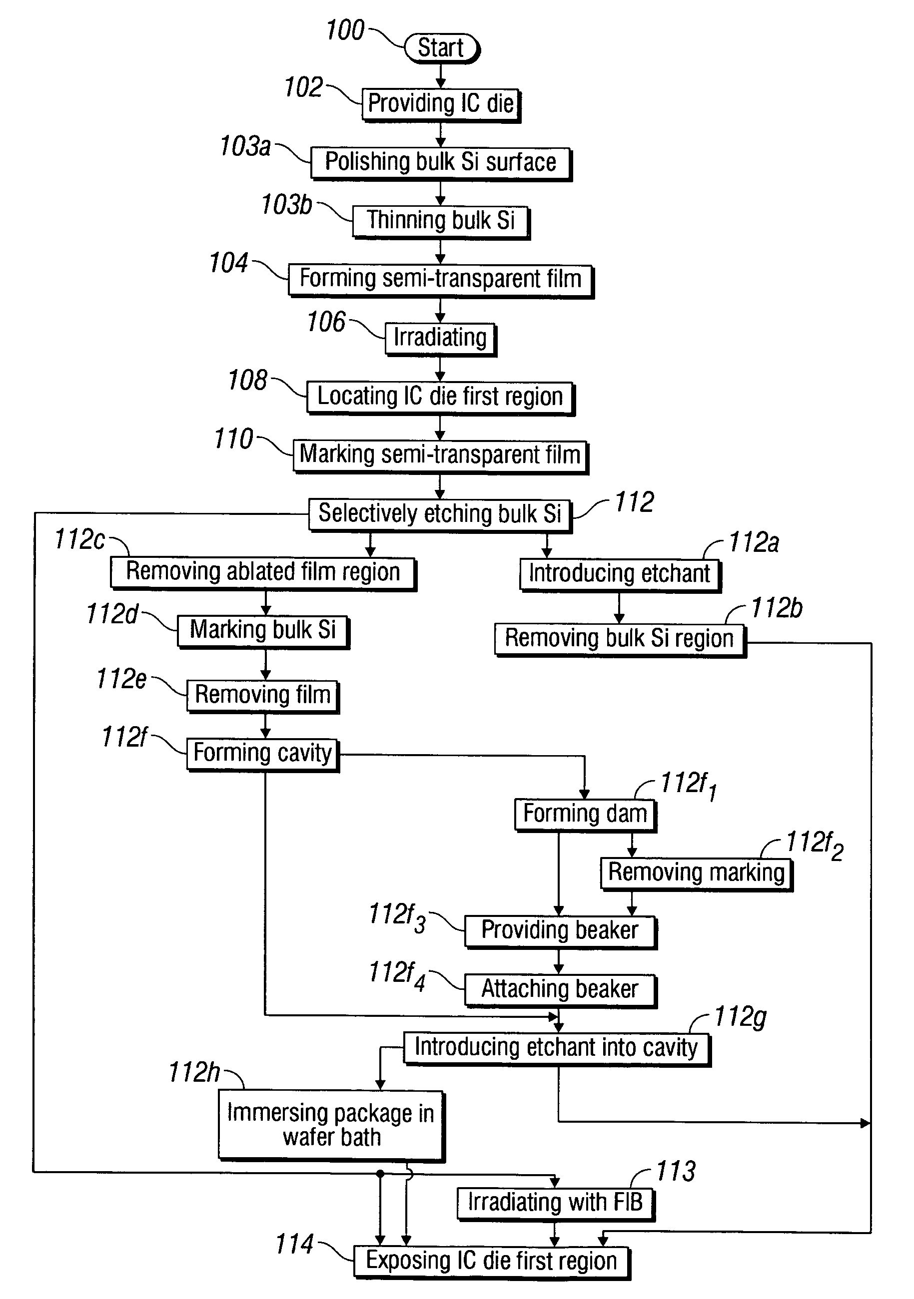
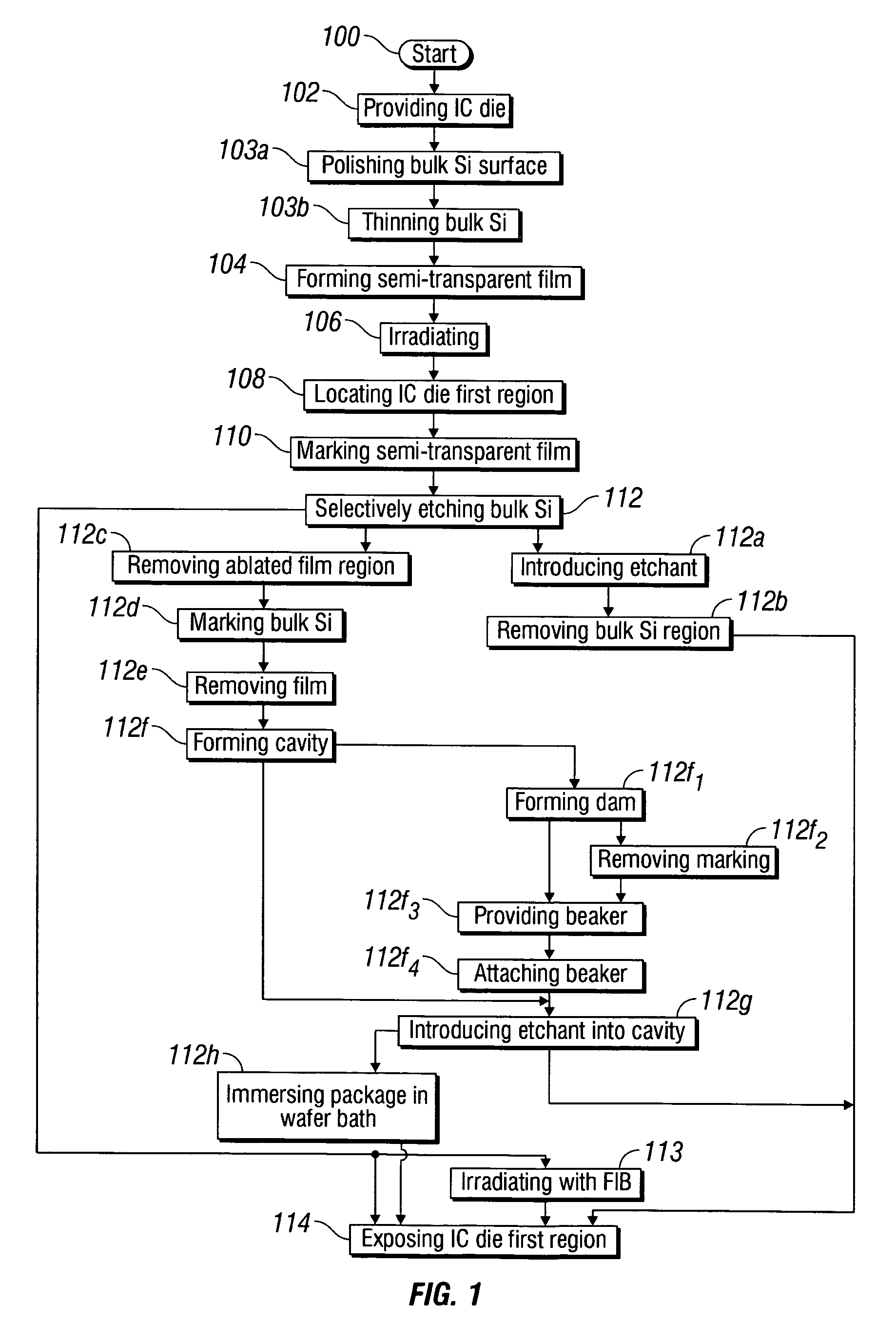
[0024]FIG. 1 is a flowchart illustrating a method for selectively marking a region of integrated circuit (IC). Although the method is depicted as a sequence of numbered steps for clarity, the numbering does not necessarily dictate the order of the steps. It should be understood that some of these steps may be skipped, performed in parallel, or performed without the requirement of maintaining a strict order of sequence. The method starts at Step 100.

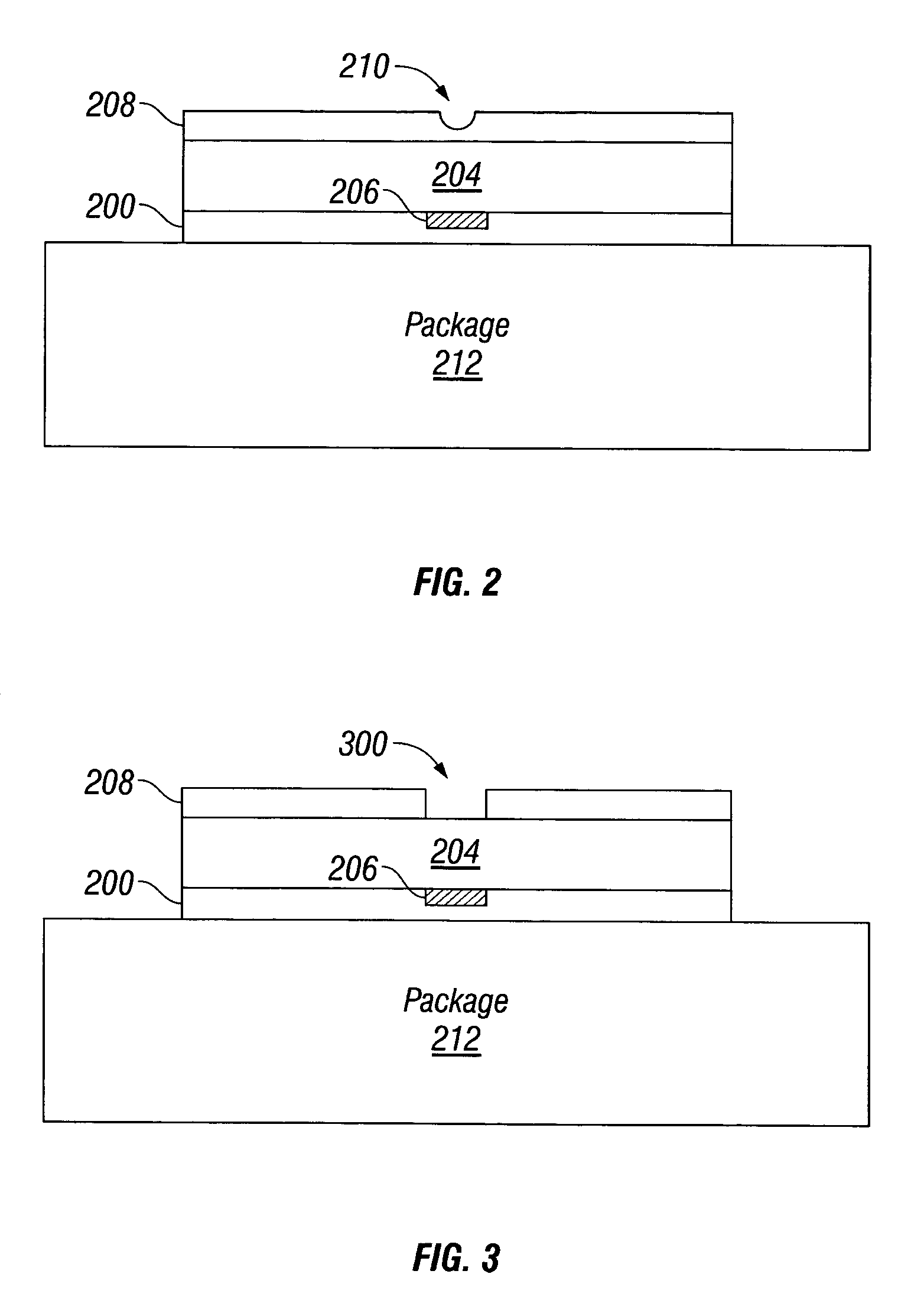
[0025]Step 102 provides an IC die with a first region located on a backside surface of a bulk silicon (Si) layer. Step 104 forms a semi-transparent film overlying the bulk Si layer, semi-transparent to light having a first wavelength. That is, the semi-transparent layer does not transmit 100% of incident light having the first wavelength. For example, the film may be semi-transparent to light having a wavelength greater than about 1 micron and less than about 2 microns. Step 106 irradiates the semi-transparent film with light having the f...


PUM


Abstract

A method is provided for selectively marking a region of integrated circuit (IC). The method provides an IC die with a first region located on a backside surface of a bulk silicon (Si) layer. A semi-transparent film is formed overlying the bulk Si layer, semi-transparent to light having a first wavelength. The semi-transparent film is irradiated with light having the first wavelength in the range of 1 to 2 microns. In response to irradiating the semi-transparent film with a first power density, the IC die first region is located. Then, in response to irradiating the semi-transparent film with a second power density, greater than the first power density, a region of the semi-transparent film is marked overlying the IC die first region. In one aspect, a region of the bulk Si layer underlying the marked (or ablated away) semi-transparent film is selectively etched to expose the IC die first region.

Description

BACKGROUND OF THE INVENTION[0001]1. Field of the Invention[0002]This invention generally relates to integrated circuits (ICs) and, more particularly, to a post-production method for selectively etching an IC, to expose regions of a fabricated IC die for investigation or repair.[0003]2. Description of the Related Art[0004]IC production facilities are established so that thousands of fragile parts can be safely processed in a short amount of time, with little human intervention. IC dice are parallel processed on a wafer, and each die may include thousands, or even millions of electrical components, such as transistors and resistors, distributed over multiple interconnected layers. Typically, an IC die is tested after fabrication, and many “internal” test points are exposed at this point in the process. After attachment to an IC package, for example using an epoxy adhesive, only the package external interfaces, or pins are accessible.[0005]While it is rarely cost effective to repair an...

Claims


Application Information

Patent Timeline
Patent Type & Authority Patents(United States)
IPC IPC(8): H01L21/336
CPCH01L23/544H01L22/14H01L2924/0002H01L2924/00
Inventor PATTERSON, JOSEPH M.
Owner QUALCOMM INC
Why Eureka
Try Eureka