Supercharge Your Innovation With Domain-Expert AI Agents!

Image sensor testing method and apparatus

a technology of image sensor and test method, applied in the direction of individual semiconductor device testing, optical radiation measurement, instruments, etc., can solve the problems of cis sensor operating with comparatively lower power consumption, higher operating speed, and performance of cis sensor relative to ccd sensor, and raise some difficult challenges in the context of constituent image sensor

Active Publication Date: 2008-08-05
SAMSUNG ELECTRONICS CO LTD
View PDF22 Cites 3 Cited by
  • Summary
  • Abstract
  • Description
  • Claims
  • Application Information

AI Technical Summary

Benefits of technology

[0079]Many features and advantages of the invention are apparent from the foregoing description. It is intended that appended claims cover all such features and advantages that fall within the scope of the invention. Further, since numerous modifications and variations will readily occur to those skilled in the art, it is not desired to limit the invention to the exact construction and operation illustrated and described. But rather, all such modifications and equivalents fall within the scope of the invention.

Problems solved by technology

However, CIS sensors operate with comparatively lower power consumption and at higher operating speeds.
That is, for many portable electronic devices constrained in their design and operating characteristics by a limited battery life, the reduced power consumption is an acceptable trade-off with the inferior performance of CIS sensors relative to CCD sensors.
This current design preference related to portable electronic devises raises some difficult challenges in the context of the constituent image sensors.
For example, given the inherent weaknesses associated with CIS sensors (e.g., high noise and less uniformity between individual sensor operations), the quality control and testing processes within the lengthy sequence of fabrication processes necessary to manufacture CIS sensors become increasingly important.
Such testing directly implicates the quality of the optical test equipment and, more particularly, the quality of the illumination source within the optical test equipment.
Without such qualities in an illumination source, it is impossible to distinguish performance variations between individual image sensors formed on the wafer.
Such an approach requires interruptions of the fabrication process, as test equipment is taken off-line for maintenance.
Unfortunately, this is almost never the case.
The difficulty of consistently providing uniform, high quality illumination sources is compounded by the fact that the performance of all illumination sources tends to degrade over time.
They do not accurately take into consideration the actual performance of individual illumination sources.
All of the foregoing results in an unacceptably high level of variation in the performance quality of illumination sources.
Absent a reliable and clearly defined optical reference signal (e.g., uniform optical energy having a well controlled intensity) it is not possible to accurately characterize the performance of individual image sensors formed on a wafer.
It is nearly impossible to identify such process variations during wafer level optical testing of image sensors if the characteristics of the illumination source in the optical test equipment also vary across the surface of the wafer.

Method used


Image

  • Image sensor testing method and apparatus
  • Image sensor testing method and apparatus
  • Image sensor testing method and apparatus

Examples


Embodiment Construction

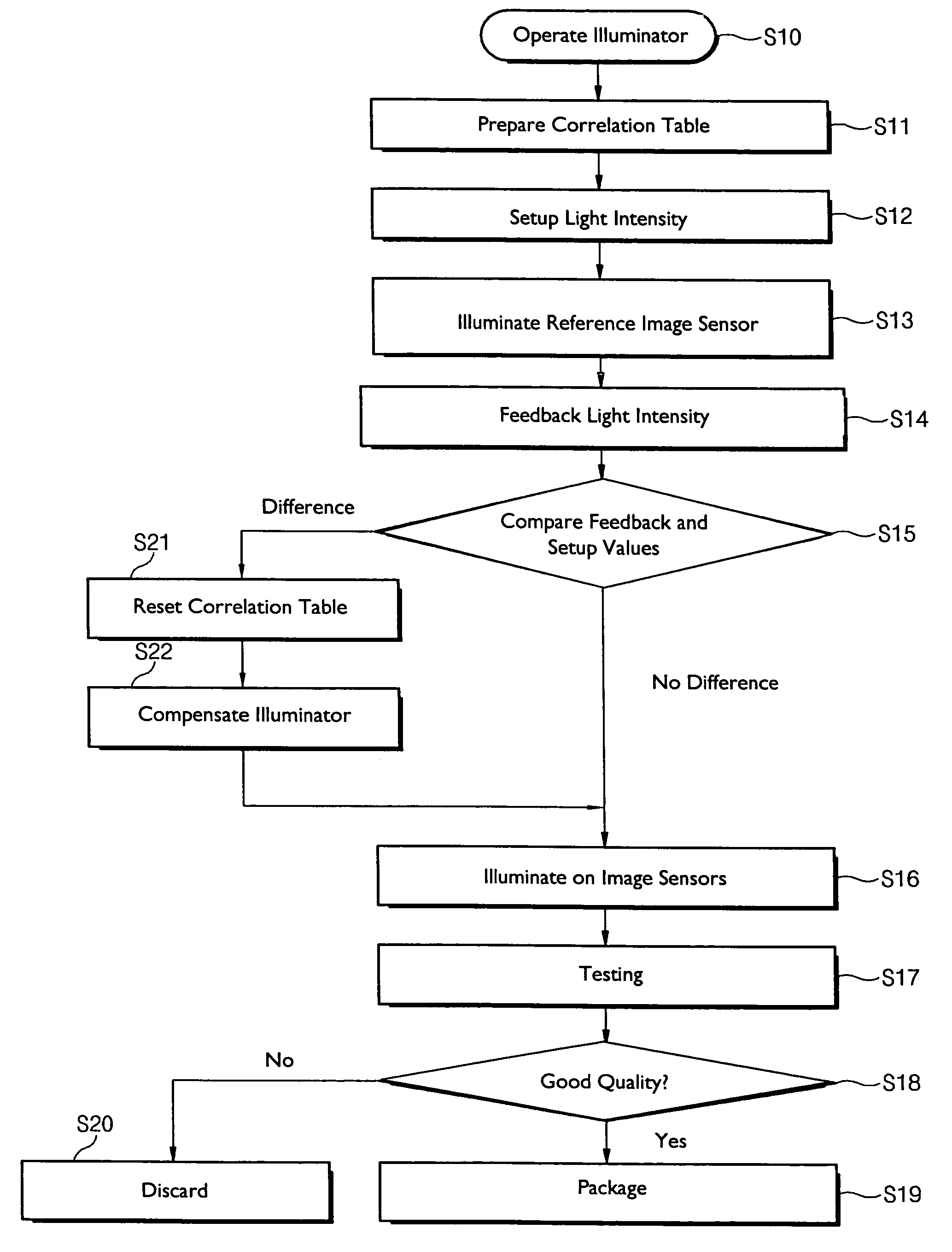
[0027]In the following description, for purposes of explanation and not limitation, embodiments of the invention are set forth to provide a more thorough understanding of the making and use of the invention. However, those of ordinary skill in the art having had the benefit of the subject disclosure will understand that other embodiments of the invention are possible. That is, numerous modifications and reconfigurations of the exemplary embodiments are possible without removing such from the scope of the appended claims. Moreover, descriptions of certain well understood aspects of the testing apparatus and related methods have been omitted for the sake of brevity.

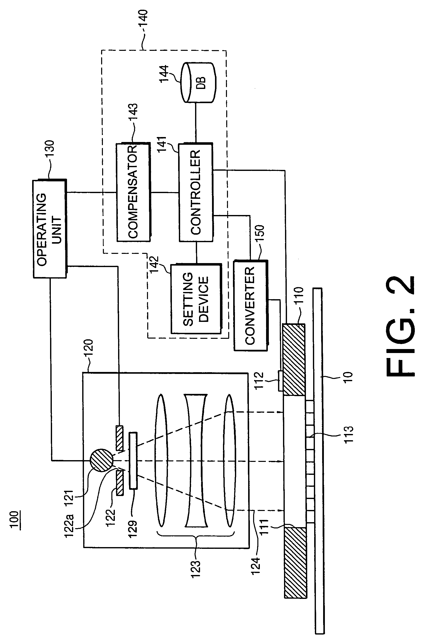
[0028]Embodiments of the invention provide an optical testing apparatus incorporating higher quality illumination sources that provide an optical test signal (e.g., collimated light) having improved uniformity and precisely controlled characteristics. Embodiments of the invention provide related optical testing methods more...


PUM


Abstract

Disclosed are an optical test apparatus, related test method and method of operation, and related probe card adapted to optically test an image sensor. An illumination source of the optical test apparatus provides an optical test signal to the image sensor through the probe card. The optical test signal has a property variably defined by a feedback loop formed between a reference image sensor associated with the probe card and a control unit connected between the reference image sensor and the illumination source.

Description

BACKGROUND OF THE INVENTION[0001]1. Field of the Disclosure[0002]Embodiments of the invention relate generally to image sensor testing methods and related testing apparatuses. More particularly, embodiments of the invention relate to automated test methods for image sensors and related test apparatuses providing improved testing uniformity.[0003]This application claims the priority of Korean Patent Application Nos. 2006-0002296, filed Jan. 9, 2006, and 2006-0022314, filed Mar. 9, 2006, the disclosures of which are hereby incorporated by reference in their entirety.[0004]2. Description of the Related Art[0005]Improved semiconductor fabrication technology has resulted in semiconductor image sensors characterized by smaller size, high quality performance, and lower manufacturing costs. As a result, image sensors are now used in a wide variety of commercial devices, such as digital cameras, camcorders, printers, scanners, and certain cellular telephones. In general operation, image sens...

Claims


Application Information

Patent Timeline
Patent Type & Authority Patents(United States)
IPC IPC(8): G01R31/302
CPCG01N21/9501G01J1/00
Inventor LEE, JONGMOONLEE, JUNTAEK
Owner SAMSUNG ELECTRONICS CO LTD
Features
  • R&D
  • Intellectual Property
  • Life Sciences
  • Materials
  • Tech Scout
  • Unparalleled Data Quality
  • Higher Quality Content
  • 60% Fewer Hallucinations
Learn More