Microprobe tips and methods for making

a technology of microprobes and tips, applied in the field of microprobes, can solve the problems of destructive separation of masking materials from substrates, and achieve the effect of reducing the risk of contamination

Active Publication Date: 2008-08-19
MICROFAB
View PDF68 Cites 41 Cited by
  • Summary
  • Abstract
  • Description
  • Claims
  • Application Information

AI Technical Summary

Problems solved by technology

The CC mask plating process is distinct from a “through-mask” plating process in that in a through-mask plating process the separation of the masking material from the substrate would occur destructively.

Method used


Image

  • Microprobe tips and methods for making
  • Microprobe tips and methods for making
  • Microprobe tips and methods for making

Examples


first embodiment

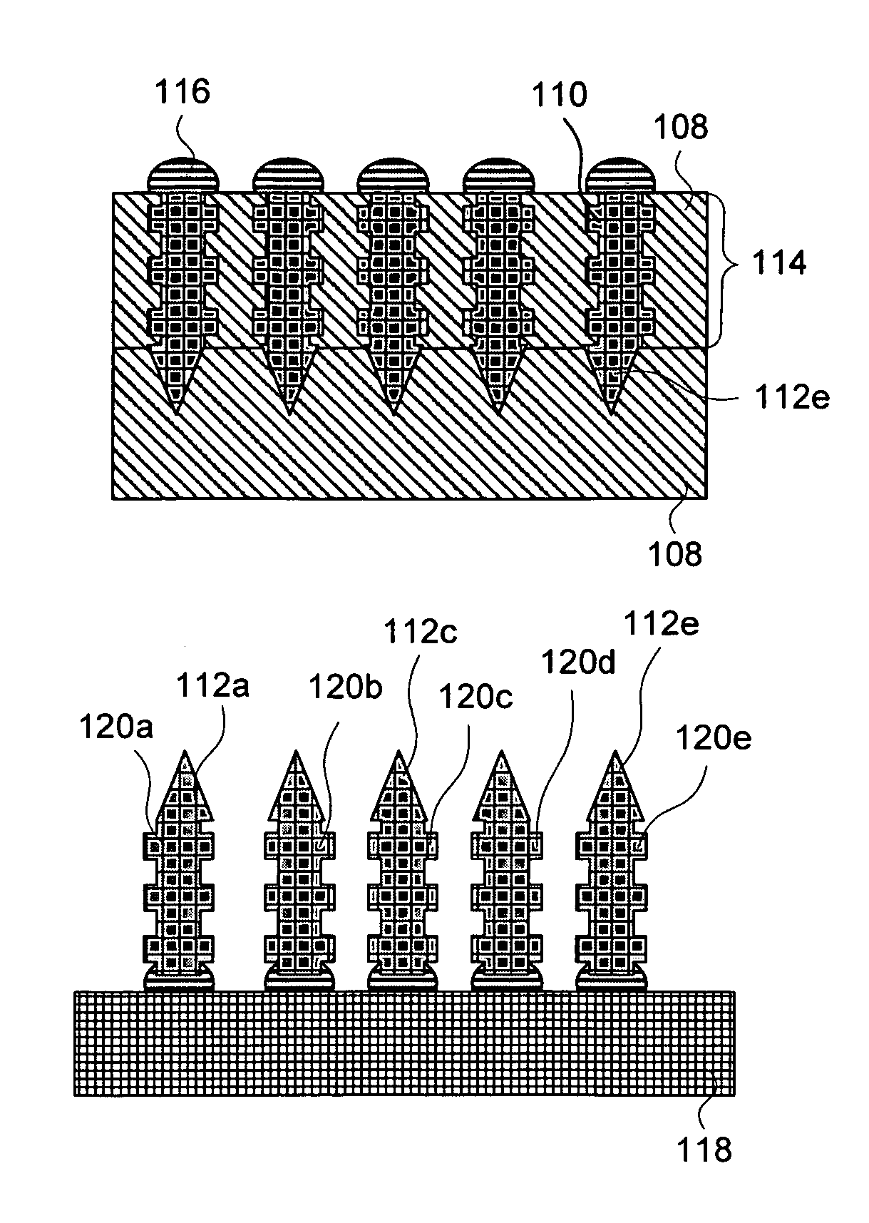
[0084]FIGS. 5A-5J schematically depict side views at various stages of the process for forming an array of probe elements according to the invention where the probe element tips are formed via electroplating onto a seed layer coated epoxy template which was molded from a silicon wafer that underwent patterned anisotropic etching.

[0085]FIG. 5A depicts a state of the process after a patterned silicon wafer is supplied. The silicon wafer has been patterned by placing a mask over its surface and patterning the mask to have openings in regions that correspond to desired probe tip locations. While the mask is in place an isotropic etching is preformed to create V-shaped or conically shaped holes in the silicon.

[0086]In alternative embodiments these openings may take the form of V-shaped trenches where it is desired that probe tips take such a form. The openings 104 and silicon 102 correspond to desired probe tip locations and represent the compliment of the probe tip shape. After the patt...

third embodiment

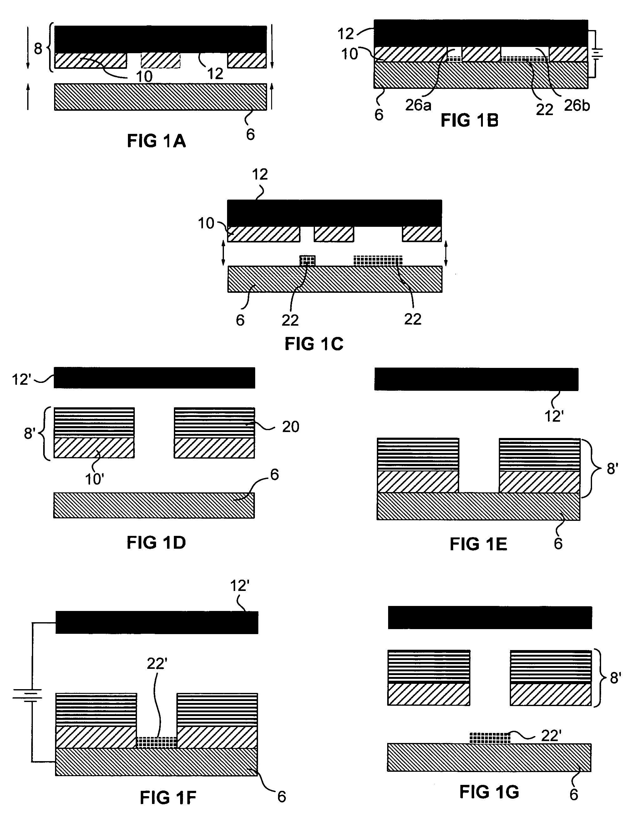
[0105]FIGS. 7A-7F schematically depict side views at various stages of a process for forming a probe element according to the invention where the probe element tip is formed using a protrusion of patterned photoresist that is made to have an undercut.

[0106]FIG. 7A depicts a state of the process where a temporary substrate 182 is coated with a negative photoresist material 184, e.g. Futurrex NR9-8000, which has one or more openings 188 through which radiation 190 may be directed to expose the photoresist material. Openings 188 correspond to locations where probe element tip material 192 will eventually be located on substrate 182.

[0107]FIG. 7B depicts a state of the process after substrate 182 and photoresist 184 have been immersed in a developing solution 194 such that unexposed portions of photoresist 184 are removed and such that exposed region 184a remains.

[0108]FIG. 7C depicts a state of the process after continuing to expose photoresist element 184a to developing solution so th...

fourth embodiment

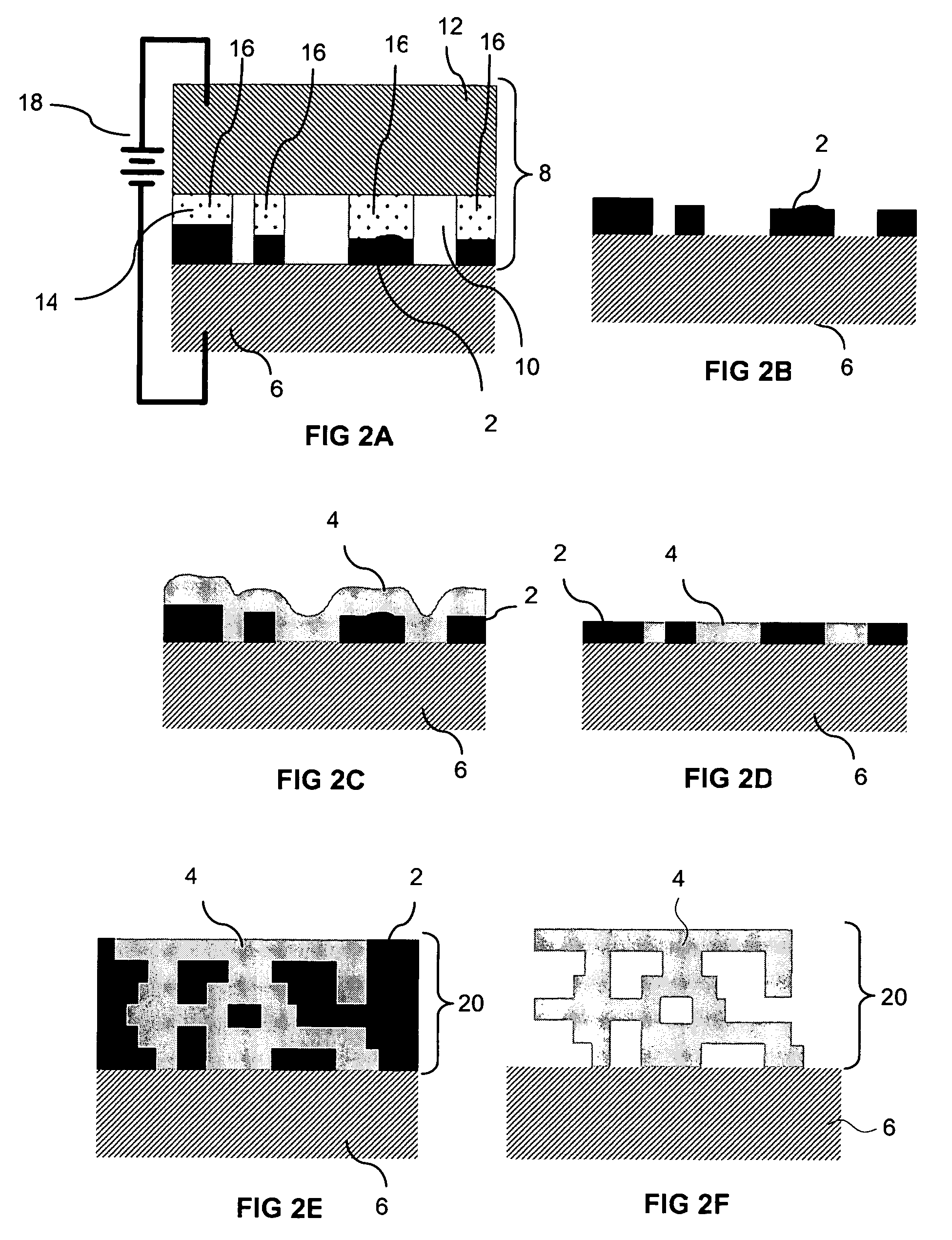
[0114]FIGS. 8A-8F schematically depict side views at various stages of a process for forming a probe element according to the invention where the probe element tip is formed using an indentation in a patterned photoresist that is made to have sidewalls that taper outward.

[0115]FIG. 8A depicts a state of the process after a temporary substrate 212 is coated with a positive photoresist 214 and a mask 216 with one or more openings 218 positioned above the photoresist. Radiation 220 is allowed to expose the photoresist in hole regions 218.

[0116]FIG. 8B depicts a state of the process after exposed photoresist 214 is developed and then overdeveloped to yield opening or openings 222 having tapered side walls 224.

[0117]FIG. 8C depicts a state of the process after a probe element tip material 226 is deposited into opening 222 of photoresist 214 and then photoresist 214 is removed.

[0118]FIG. 8D depicts a state of the process after a sacrificial material 228 is electrodeposited over substrate ...


PUM

PropertyMeasurementUnit
angleaaaaaaaaaa
shapeaaaaaaaaaa
conductiveaaaaaaaaaa

Abstract

Embodiments of the present invention are directed to the formation of microprobe tips elements having a variety of configurations. In some embodiments tips are formed from the same building material as the probes themselves, while in other embodiments the tips may be formed from a different material and / or may include a coating material. In some embodiments, the tips are formed before the main portions of the probes and the tips are formed in proximity to or in contact with a temporary substrate. Probe tip patterning may occur in a variety of different ways, including, for example, via molding in patterned holes that have been isotropically or anisotropically etched silicon, via molding in voids formed in over exposed photoresist, via molding in voids in a sacrificial material that have formed as a result of the sacrificial material mushrooming over carefully sized and located regions of dielectric material, via isotropic etching of a the tip material around carefully sized placed etching shields, via hot pressing, and the like.

Description

RELATED APPLICATIONS[0001]This application claims benefit of U.S. Application Nos. 60 / 533,975, filed Dec. 31, 2003; 60 / 540,510, filed Jan. 29, 2004; 60 / 533,933, filed Dec. 31, 2003; 60 / 536,865, filed Jan. 15, 2004; 60 / 540,511, filed Jan. 29, 2004. Each of these applications is incorporated herein by reference as if set forth in full herein including any appendices attached thereto.FIELD OF THE INVENTION[0002]The present invention relates generally to microprobes (i.e. compliant contact elements) and EFAB™ type electrochemical fabrication processes for making them and more particularly to microprobe tips designs and process for making them.BACKGROUND[0003]A technique for forming three-dimensional structures (e.g. parts, components, devices, and the like) from a plurality of adhered layers was invented by Adam L. Cohen and is known as Electrochemical Fabrication. It is being commercially pursued by Microfabrica Inc. (formerly MEMGen® Corporation) of Burbank, Calif. under the name EFAB...

Claims


Application Information

Patent Timeline
Patent Type & Authority Patents(United States)
IPC IPC(8): H01R43/02H01R9/00G01R31/02H01R12/00H01R13/187H01R24/58
CPCG01R1/0483G01R1/06716G01R1/07357G01R31/2886Y10T29/49213Y10T29/49208Y10T29/49204Y10T29/49149Y10T29/49147Y10T29/49211Y10T29/4921
Inventor KIM, KIEUNCOHEN, ADAM L.LARSEN, WILLA M.CHEN, RICHARD T.KUMAR, ANANDA H.KRUGLICK, EZEKIEL J. J.ARAT, VACITZHANG, GANGLOCKARD, MICHAEL S.
Owner MICROFAB
Why Eureka
Try Eureka