Method of fabricating gate of fin type transistor

a transistor and gate technology, applied in the direction of semiconductor devices, basic electric elements, electrical appliances, etc., can solve the problems of defective device operation, difficult to precisely control the width of the recess, and difficult to prevent etch damage to the silicon oxide layer in the device isolation region

Active Publication Date: 2008-08-19
SAMSUNG ELECTRONICS CO LTD
View PDF5 Cites 16 Cited by
  • Summary
  • Abstract
  • Description
  • Claims
  • Application Information

AI Technical Summary

Benefits of technology

[0012]According to embodiments of the invention, a method of fabricating a gate of a fin type transistor precisely controls the width of a recess exposing both sidewalls of an active region when the recess is formed using a damascene process.

Problems solved by technology

Hence, it is often very difficult to prevent etch damage to the silicon oxide layer in the device isolation regions, for example, which mainly includes a silicon oxide layer.
As a result, it is also difficult to precisely control the widths of the recesses.
However, if the widths of the recesses are larger than the initially determined widths of the recesses, a bridge may be formed between the gate lines, resulting in defective device operation.

Method used


Image

  • Method of fabricating gate of fin type transistor
  • Method of fabricating gate of fin type transistor
  • Method of fabricating gate of fin type transistor

Examples


Embodiment Construction

[0016]The invention will now be described more fully with reference to the accompanying drawings, in which exemplary embodiments of the invention are shown. The invention may, however, be embodied in many different forms and should not be construed as being limited to the embodiments set forth herein; rather, these embodiments are provided so that this disclosure will be thorough and complete, and will fully convey the concept of the invention to those skilled in the art.

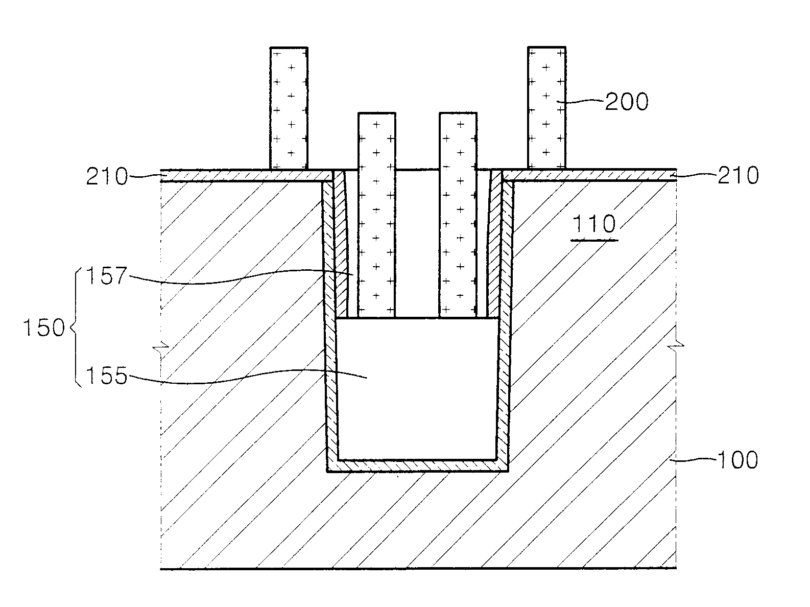
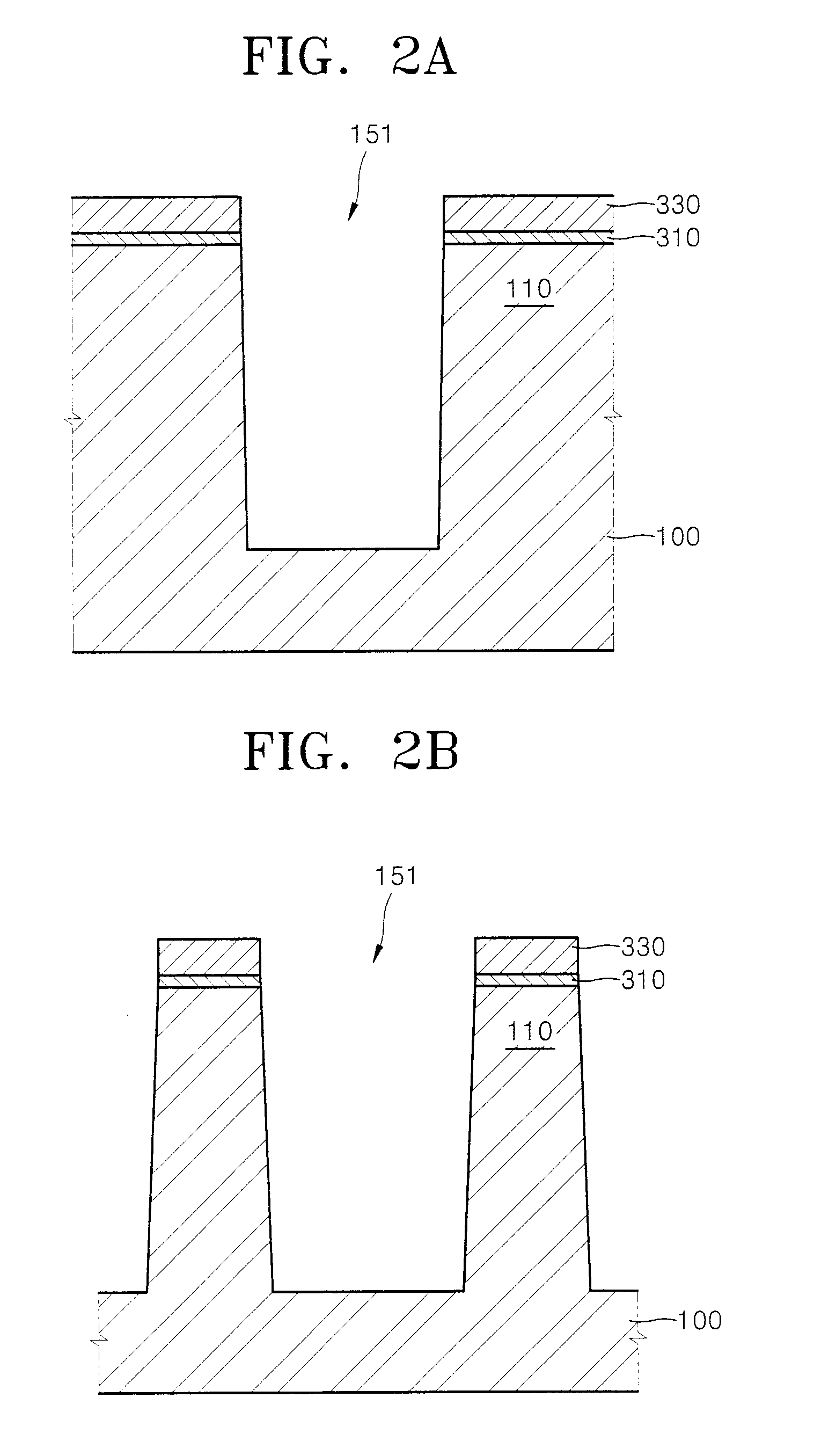
[0017]According to one exemplary embodiment of the invention, a device isolation region defining active regions is formed, for example, by performing a shallow trench isolation (STI) process. Also, in the present exemplary embodiment, prior to forming a plurality of recesses that expose sidewalls of the active regions to the device isolation region, sidewall protection layers, which can protect the sidewalls of the active regions from subsequent processes, are formed. The sidewall protection layers may be formed as ...


PUM


Abstract

A method of fabricating a gate of a fin type transistor includes forming hard masks to define active regions of a substrate. A shallow trench isolation method is performed to form a first device separation layer, and then an etch-back process is performed such that the active regions protrude. Sidewall protection layers are formed on sidewalls of the active region, and a second device separation layer is formed thereon, thereby obtaining a device isolation region. The sidewall protection layers include an insulation material with an etch selectivity with respect to an insulation material composing the device isolation region. The device isolation region is selectively etched to form recesses for a fin type active region. Dry etching and wet etching are performed on the silicon nitride to remove the hard masks and the sidewall protection layers, respectively. Gates are formed to fill the recesses.

Description

CROSS-REFERENCE TO RELATED APPLICATIONS[0001]This application claims priority from Korean Patent Application No. 10-2005-0069142, which was filed on 28 Jul. 2005. Korean Patent Application No. 10-2005-0069142 is incorporated by reference in its entirety.BACKGROUND[0002]1. Field of the Invention[0003]This disclosure relates to manufacturing techniques for semiconductor devices, and more particularly, to a method of fabricating a gate of a fin type transistor.[0004]2. Description of the Related Art[0005]Semiconductor devices are becoming more highly integrated and can be operated at lower power and at higher speed. Particularly, methods have been developed to prevent a short channel effect and improve device reliability. A fin type transistor such as FinFET (Fin Field Effect Transistor) formed using such a method has been introduced to enhance a current characteristic.[0006]A fin type transistor includes a fin type active region. Both sidewalls of the fin type active region can be use...

Claims


Application Information

Patent Timeline
Patent Type & Authority Patents(United States)
IPC IPC(8): H01L21/336H01L31/062
CPCH01L21/823412H01L29/66795H01L21/823437H01L29/7851H01L21/76224H01L21/76283
Inventor KIM, YONG-SUNGCHUNG, TAE-YOUNGSHIN, SOO-HO
Owner SAMSUNG ELECTRONICS CO LTD
Why Eureka
Try Eureka