Processes for making reliable VCSEL devices and VCSEL arrays

a technology of vcsel devices and arrays, applied in the direction of lasers, semiconductor laser structural details, semiconductor lasers, etc., can solve the problems of affecting stable operation and reliability, inducing strain in epitaxial layers and also between, and designing a process applicable in the manufacturing environment for high volume and large area wafers is particularly challenging, so as to reduce overall stress, reduce the total volume of the oxide zone, and reduce the overall volume

Active Publication Date: 2016-12-13
PRINCETON OPTRONICS
View PDF13 Cites 12 Cited by
  • Summary
  • Abstract
  • Description
  • Claims
  • Application Information

AI Technical Summary

Benefits of technology

[0021]In this invention a process to fabricate a VCSEL device wafer with significantly improved reliability is provided. In one embodiment of the invention a strain compensating film is provided. More specifically the strain compensating film on the semiconductor wafer to counteract significant bowing and / or warping in the wafer which is induced due to strain in multiple epitaxial layers.
[0024]The oxidation process provides good control over the oxidation rate to precisely control the width of the aperture. In a variant aspect the width of the aperture is limited to about 10 micrometer or less so as to minimize the total volume of the oxide zone. The wafers during oxidation are heated and cooled at slow rates to reduce overall stress. In one aspect the heating and cooling rates are set to about 20° C. / min. or lower, respectively.
[0025]A further process step in the oxidization process that improves the long term reliability is to remove as much as possible the moisture present in the oxidized semiconductor, after the oxidation process. Moisture is introduced in the oxide during the oxidation process which uses water vapor.
[0026]In another aspect of the invention in the reduction of the bowing and / or warping of the VCSEL device wafer by incorporating the strain compensation film provides significant improvement in overall stress reduction in a number of process following the fabrication of VCSEL device wafer. The improvements are observed in the processes of lithography, mesa construction, thinning of the wafer for ultrathin VCSEL wafers, metallization, bonding to a submount for heat dissipation. In a different aspect additional reliability improvement is provided by a low temperature metallization process for constructing electrical contacts to the VCSEL devices.
[0027]In a variant aspect, an etching process is used for dicing the wafers instead of traditional method of sawing, thereby reducing overall stress of the VCSEL device wafer and improving reliability. The etching process for dicing includes Reactive Ion Etching (RIE), Inductively Coupled Plasma (ICP) etching. chemical etching or a combination of these processes.
[0028]The application of some or all of these fabrication processes and / or improvements has facilitated reducing overall stress and increased the performance of the VCSELs and VCSEL arrays and increased the long-term reliability by more than a factor of 20.

Problems solved by technology

Therefore, designing a process applicable for high volume and large area wafers in manufacturing environment is particularly challenging due to stress arising from one or more process steps including growth of large number of epitaxial layers.
The strain in the active region may generate defects and / or dislocations in the resulting structure which affect stable operation and reliability.
These structural modifications which are critical for intended device operation, results in inducing strain in the epitaxial layers and also between the epitaxial layers and the substrate wafer.
Thus significant bowing and / or warping of the wafer (including the epitaxial layers) may occur, which not only induces strain in the device but lack of flatness is particularly detrimental for some critical processing steps for example lithography, on a large area and / or thin substrates used in a manufacturing environment, and therefore impacts yield.
However, the process introduced other defects that compromise device performance.
Furthermore, incorporating an appropriately designed strain compensation layer on the substrate on a surface opposite to the epitaxial layer structure is not considered or incorporated in the design of a fabrication process before.
One important drawback of oxide apertures arises from the volume of oxide present in the VCSEL device that may introduce stress and affect reliability.
However, a large volume of oxide grown to reduce the aperture diameter to a required size as compared to the mesa diameter may result in significant difference in thermal expansion rates of the VCSEL epitaxial layers and the oxide region, causing stress and thereby affecting reliability.
Current confinement aperture constructed by oxidation has a second detrimental aspect.
Operation of VCSEL devices particularly at high power levels creates significant heat in the device.
Therefore optimum operation requires VCSELs to be designed with high thermal conductivity to dissipate heat which would otherwise limit performance and output power of the VCSEL.
However, high temperature process can introduce defects into the device and potentially degrade the properties of the device structure fabricated in earlier process steps.
The dicing saw or even the dicing scribe has the potential to create crystal defects which can then propagate into the epitaxial region of the VCSEL device or arrays of devices.
These defects may affect one or more properties of the VCSEL epitaxial layers thereby reducing inherent gain of the device causing optical loss and impacting long term stability and reliability.
Although many process steps for constructing of VCSEL devices are well known, and have been optimized for smaller size wafers and for particular material systems, applying same process steps to large size wafers and / or to thin wafers is particularly challenging because bowing and / or warping of wafers may be sufficiently large to affect the flatness of the wafer in subsequent post epitaxial layer growth processing steps, for example, while performing critical alignment steps such as lithography, substrate thinning / removal, metallization, etc.
In addition, wafer bowing and / or warping is particularly detrimental in bonding the finished VCSEL device to a submount including a thermal submount or a printed circuit board with or without a region for efficient heat dissipation, which affects the performance of high power VCSEL devices in particular.
Efficient heat dissipation is only possible if the VCSEL device is positioned flat and in close contact with the submount.
In case of a thin wafer the bowing may even cause breakage thereby resulting in poor yield.
Standard prior art VCSEL device processing methods are quite advanced, but still do not address or provide a solution to this important issue of bowing and / or warping which poses challenges in adapting standard VCSEL device processing on a large area wafer particularly for large scale manufacturing environment.
There are many steps that may introduce stress in the structure which degrades performance and ultimately compromises reliability and leads to device failure.

Method used


Image

  • Processes for making reliable VCSEL devices and VCSEL arrays
  • Processes for making reliable VCSEL devices and VCSEL arrays
  • Processes for making reliable VCSEL devices and VCSEL arrays

Examples


Embodiment Construction

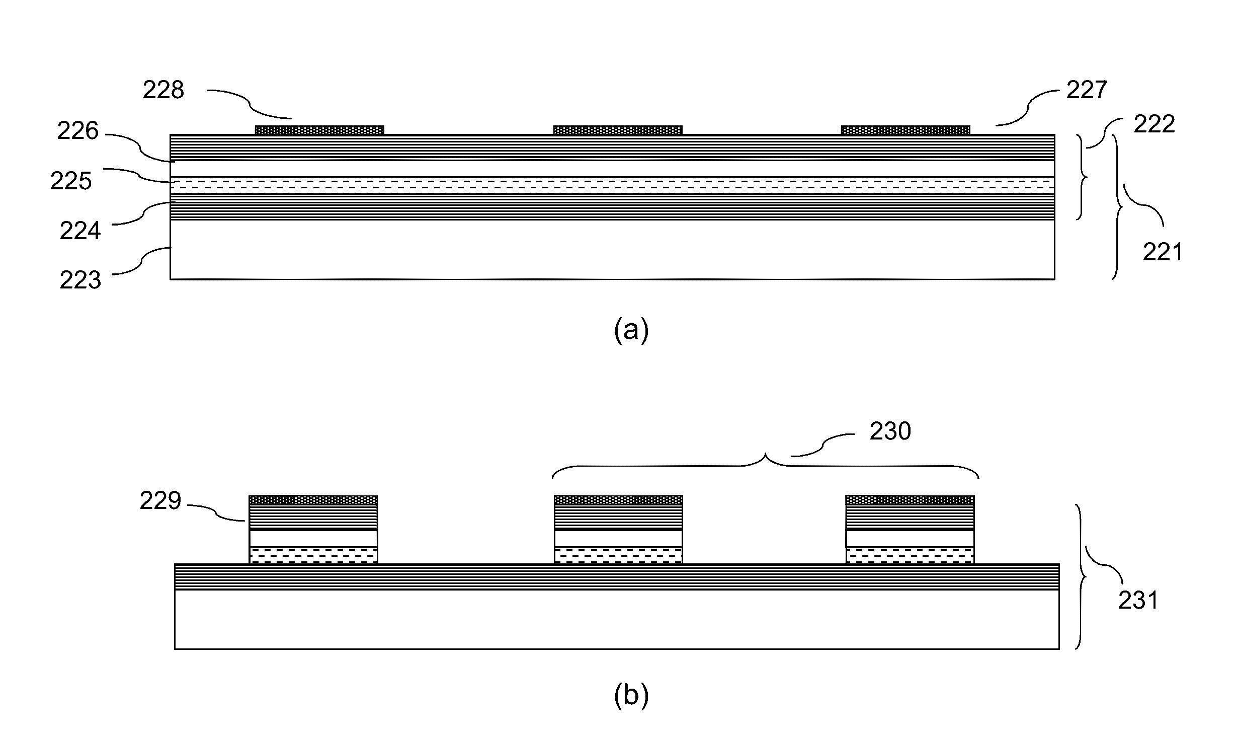
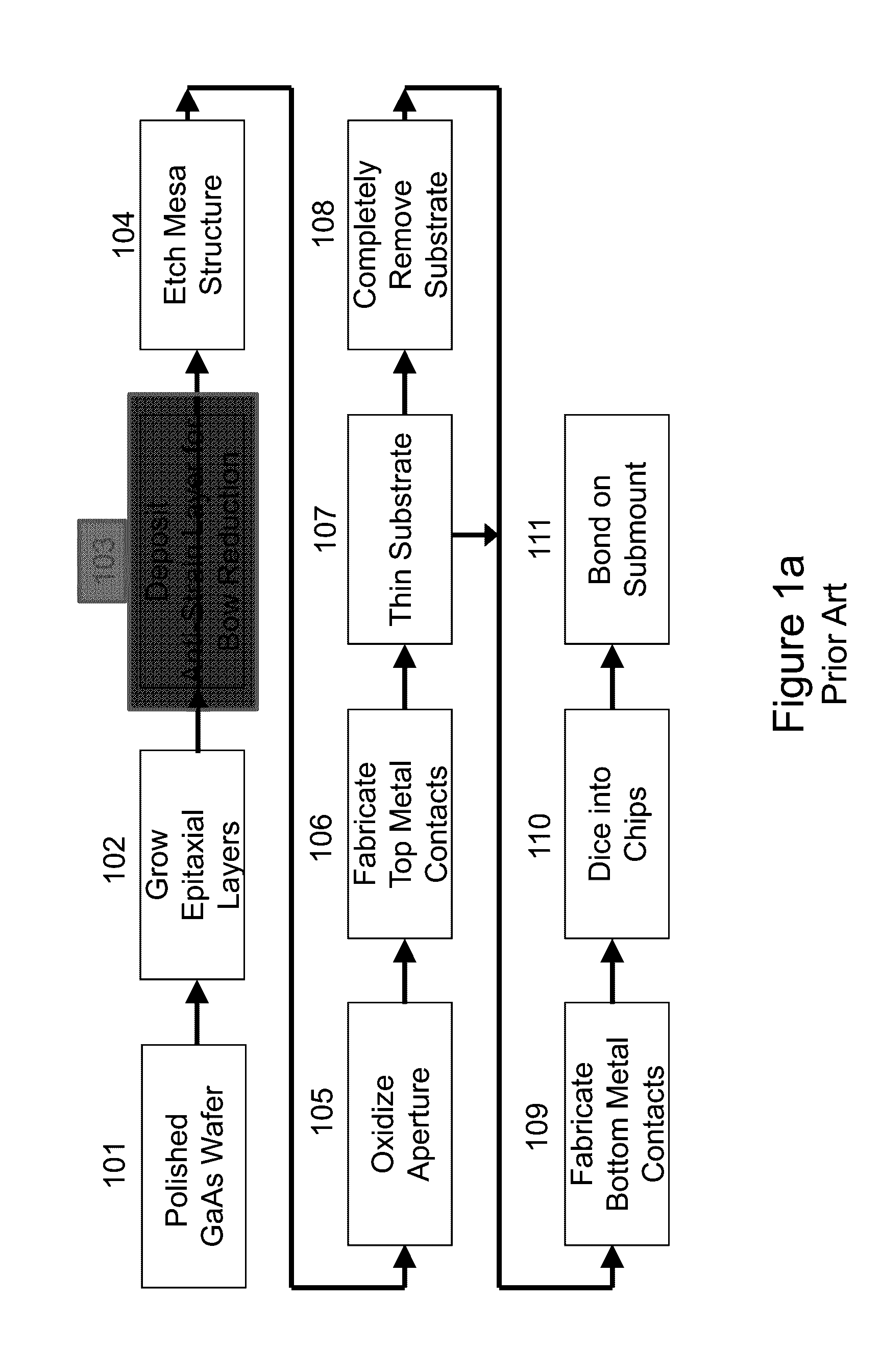
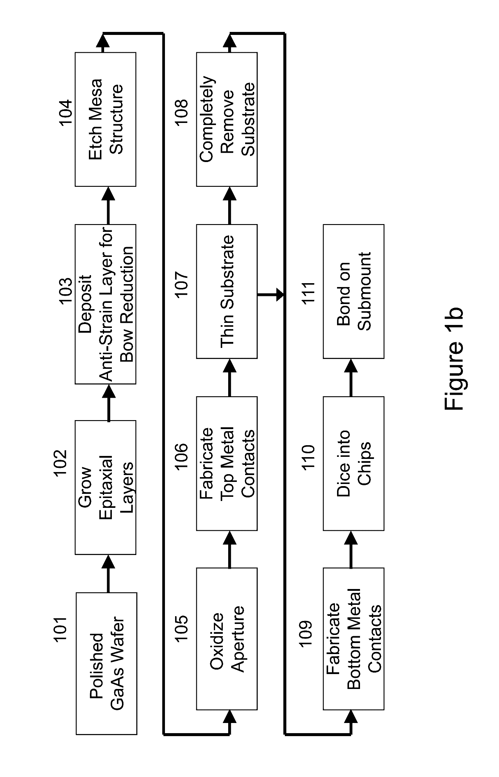
Basic Process to Construct VCSEL Device

[0042]A broad framework of the principles will be presented by describing various aspects of this invention using exemplary embodiments and represented in different drawing figures. While the drawing figures show a structure, the structure is used to illustrate / describe a process that is used to create the structure. The process in this context is used synonymous to a method or a step in a sequence of processes that need to be carried out in a particular order to achieve a certain beneficial result for a given structure of a VCSEL device. For clarity and ease of description, each embodiment includes only a few aspects. Different aspects from different embodiments may be combined or practiced separately, to design a customized process depending upon application requirements. Many different combinations and sub-combinations of few representative processes shown within the broad framework of this invention, that may be apparent to those skilled in...


PUM


Abstract

A set of VCSEL fabrication methods has been invented which enhance the performance and long time reliability of VCSEL devices and arrays of devices. Wafer bow caused by growing a large number of epitaxial layers required to fabricate VCSEL device generates strain and results in bowing / warping of the device wafer. The stress so generated is eliminated by applying a stress compensation layer on the substrate to a surface opposite to the epitaxial layer surface. New oxidation equipment designs and process parameters are described which produce more precision apertures and reduce stress in the VCSEL device. An ultrathin fabrication procedure is described which enables high power VCSELs to be made for high power operation at many different wavelengths. A low temperature electrical contacting process improves VCSEL long term reliability.

Description

CROSS REFERENCE TO RELATED APPLICATION[0001]This application claims priority benefit from the U.S. Provisional Patent Application No. 61 / 947,723 filed on Mar. 4, 2014, the contents of which is being incorporated by reference in their entirety.BACKGROUND OF THE INVENTION[0002]Field of Invention[0003]This invention relates to a method and in particular, to a sequence of fabrication steps for constructing semiconductor lasers, and in particular, vertical cavity surface emitting lasers (VCSELs) and arrays of VCSELs, exhibiting long term stability and reliability.[0004]Background Art[0005]The fabrication processes for making VCSELs involve a series of steps as shown in a process flow diagram shown in FIG. 1. A VCSEL or VCSEL arrays (synonymously referred as VCSEL devices hereinafter) are grown on a semiconductor substrate and in general, includes steps of one or more layers of epitaxial crystal growth, growth or deposition of different materials to facilitate etching of layers, lithograp...

Claims


Application Information

Patent Timeline
Patent Type & Authority Patents(United States)
IPC IPC(8): H01L21/00H01S5/022H01S5/183H01S5/042H01S5/42H01S5/02
CPCH01S5/0224H01S5/18305H01S5/18311H01S5/18347H01L2224/48091H01L2224/73265H01S5/0203H01S5/0217H01S5/0425H01S5/423H01L2924/00014H01S5/0207H01S5/02469H01S5/0234H01S5/02345
Inventor WANG, QINGSEURIN, JEAN-FRANCOISGHOSH, CHUNI LWATKINS, LAURENCE S
Owner PRINCETON OPTRONICS
Why Eureka
Try Eureka