Laser modulating and driving device and image reproducing apparatus using the same

a technology of laser modulation and driving device, applied in the direction of electrographic process, electrographic process using charge pattern, instruments, etc., can solve the problems of increasing data lines, increasing complexity, and increasing the structure of data transmission part and transmission path, so as to reduce energy change, improve the accuracy of pulse width, and improve the effect of durability

Inactive Publication Date: 2009-02-24
RICOH KK
View PDF17 Cites 15 Cited by
  • Summary
  • Abstract
  • Description
  • Claims
  • Application Information

AI Technical Summary

Benefits of technology

[0015]It is still another object of the invention to eliminate the inconsistency between increased supply voltage for driving a laser and reduced supply voltage for generating LD modulation signals.
[0016]To achieve the object, a pixel data generating unit and a modulation signal generating unit are arranged together in the same substrate (such as PCB or in the same ASIC), while a laser driving unit is placed near a light source (such as a laser). This arrangement allows a plurality of pixel data signals to be transmitted in parallel on the PCB or ASIC. At the same time, the laser driving unit arranged near the laser can achieve a high-speed laser driving characteristic.
[0021]With this laser modulating and driving device, the modulation signals are transmitted, maintaining a precise pulse width, because the small swing differential signal has less energy change and more durability against disturbance. Accordingly, high-speed driving operation is achieved, while the EMI (electromagnetic interference) characteristic and the anti-noise characteristic are improved under the precise control of laser modulation.
[0022]Since the small swing differential modulation signal allows the distance between the modulation signal generating unit and the laser driving unit to be increased, the laser driving unit can be mounted on an independent circuit board, or formed as an independent integrated circuit, separately from the modulation signal generating unit. Consequently, a sufficient supply voltage can be supplied to the laser driving unit, while high-density and low-power devices can be used in the modulation signal generating unit to produce a high-speed modulation signal, regardless of the laser driving voltage.

Problems solved by technology

The number of data lines increases and the size and the structure of the data transmission part become large and complicated, which makes it difficult to realize high-speed transmission of 64 data signals.
If such digital pixel signals are supplied from the pixel data generating unit 1110 to the LD modulation signal generating unit 1120 by differential transmission, the structure of the data transmission part and the transmission path becomes larger and more complicated.
Another problem is inconsistency in conditions of a supply voltage for laser driving and a supply voltage for generation of modulation signals.
Thus, inconsistency between the power supply voltage condition for laser driving and that for modulation signal generation becomes conspicuous.

Method used


Image

  • Laser modulating and driving device and image reproducing apparatus using the same
  • Laser modulating and driving device and image reproducing apparatus using the same
  • Laser modulating and driving device and image reproducing apparatus using the same

Examples


first embodiment

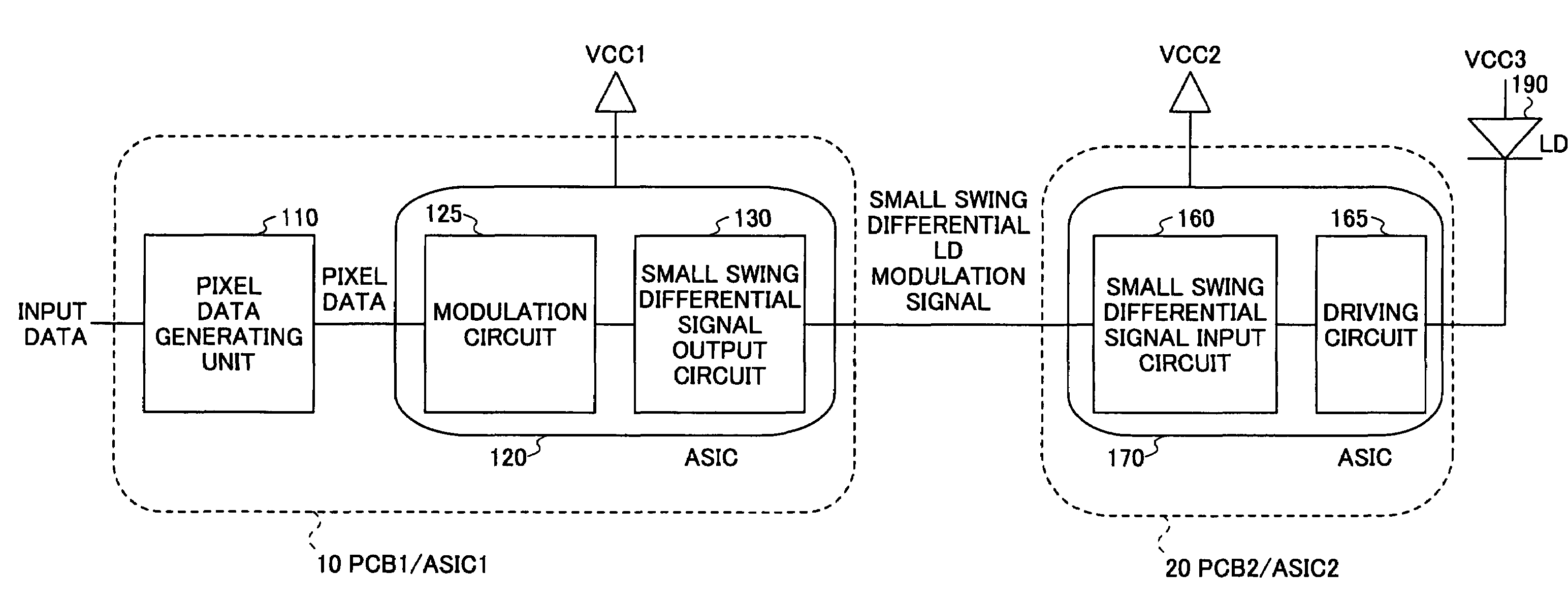
[0113]Next, the first embodiment that uses CML or ECL for producing a small swing differential signal is explained with reference to FIG. 14 through FIG. 44. In the following examples, a small swing output is produced by a single inverter; however, the same applies to the structure using multiple inverters or a buffer.

[0114]FIG. 14 is a circuit diagram of current mode logic (CML) used in the small swing output circuit 132 shown in FIG. 9A. A pair of differential signals consisting of a non-inverted LD modulation signal and an inverted LD modulation signal are input to the gates of transistors TR1 and TR2, respectively, and load resistors R1 and R2 are inserted in the CML. This arrangement makes the amplitude of the output of the CML smaller than VCC. The output level of the small swing signal can be regulated by adjusting the resistance values of the resistors R1 and R2.

[0115]FIG. 15 shows another example of producing a small swing signal pair, in which emitter coupled logic (ECL) i...

second embodiment

[0139]In FIG. 36, the output stage (i.e., the small swing output circuit 132 in this example) of the small swing differential signal output circuit 130 is formed by a CML or ECL circuit in order to achieve high speed signal transmission. Of course, the output stage of the small swing differential signal output circuit 130 may be formed of a LVDS circuit, as will be described in the

[0140]FIG. 37 shows another example of the interface between the small swing differential signal output circuit 130 and the small swing differential signal input circuit 160. The output stage of the small swing differential signal output circuit 130 is formed by a CML or ECL circuit with a supply voltage VCC1, and the small swing differential signal input circuit 160 is formed of a circuit of a different type (for example, an LVDS or ECL type) from that of the output stage of the small swing differential output circuit 130, with a supply voltage of VCC2. VCC1 is set to 1.8 V, and VCC2 is set to 5 V, for ex...


PUM


Abstract

A laser modulating and driving device comprises a modulation signal generating unit configured to generate a laser modulation signal consisting of a pair of small swing differential signals based on pixel data, and a driving unit configured to drive a laser according to the laser modulation signal supplied from the modulation signal generating unit.

Description

BACKGROUND OF THE INVENTION[0001]1. Field of the Invention[0002]The present invention generally relates to a laser driving technique used in an image reproducing apparatus, and more particularly, to a laser modulating and driving device that produces a pair of small swing differential modulation signals to drive a laser diode (LD) used as a light source in an image reproducing apparatus.[0003]2. Description of Related Art[0004]In general, a semiconductor laser (LD) or a semiconductor laser array (LD array) is used as a light source of image reproducing apparatuses, including laser printers, optical recorder / players, digital photocopying machines, and optical communication apparatuses.[0005]There are several methods for modulating the optical output of a semiconductor laser. For instance, power modulation for modulating the light quantity itself, pulse width modulation for modulating the light emitting time, and a combination of the power modulation and the pulse width modulation are...

Claims


Application Information

Patent Timeline
Patent Type & Authority Patents(United States)
IPC IPC(8): H01S3/00B41J2/47H04N1/40
CPCH04N1/40037
Inventor ISHIDA, MASAAKINIHEI, YASUHIROOMORI, ATSUFUMIOZASA, DAN
Owner RICOH KK
Why Eureka
Try Eureka