Source follower circuit or bootstrap circuit, driver circuit comprising such circuit, and display device comprising such driver circuit

a follower circuit and source circuit technology, applied in static indicating devices, instruments, optics, etc., can solve the problems of large power supply voltage and power consumption, variable threshold voltage of tft in analog buffer circuits, etc., and achieve low power supply voltage and low power consumption.

Active Publication Date: 2007-04-17
SEMICON ENERGY LAB CO LTD
View PDF27 Cites 17 Cited by
  • Summary
  • Abstract
  • Description
  • Claims
  • Application Information

AI Technical Summary

Benefits of technology

[0022]As described above, a large liquid crystal display device is required to be driven by the line sequential drive; therefore, an analog buffer circuit is required to be formed. In particular, using a polycrystalline silicon TFT can realize an integration of a pixel portion and a driver circuit, that is an analog buffer circuit. As an advantage of the integrated liquid crystal display is a low power consumption, increase in power supply voltage as described above is a serious problem.
[0025]A depletion mode polycrystalline silicon TFT (hereinafter referred to as a depletion mode TFT) has a threshold voltage on its negative voltage side. Therefore, a voltage (VGS) between the gate and source of the depletion mode TFT is approximately 0 to 1 V, which does not require an increase in an input voltage as described above. As a result, a power supply voltage does not have to be increased either, thus a low power consumption of a liquid crystal display device can be realized.
[0031]According to the invention as described above, a driver circuit using a polycrystalline silicon TFT can be operated without increasing a power supply voltage than the desired value. As a result, power supply voltage can be maintained low and a low power consumption can be realized in a display device such as a liquid crystal display device having the driver circuit of the invention, a display device having a light emitting element (referred to as a light emitting device), and a semiconductor integrated circuit such as a CPU or a memory.

Problems solved by technology

However, there is another problem besides the variation in the threshold voltage of TFT in the analog buffer circuit.
As a result, a power supply voltage as well as a power consumption becomes large while generating heat.

Method used


Image

  • Source follower circuit or bootstrap circuit, driver circuit comprising such circuit, and display device comprising such driver circuit
  • Source follower circuit or bootstrap circuit, driver circuit comprising such circuit, and display device comprising such driver circuit
  • Source follower circuit or bootstrap circuit, driver circuit comprising such circuit, and display device comprising such driver circuit

Examples


embodiment mode 1

[0039]A source follower circuit using a depletion mode TFT is described in this embodiment mode.

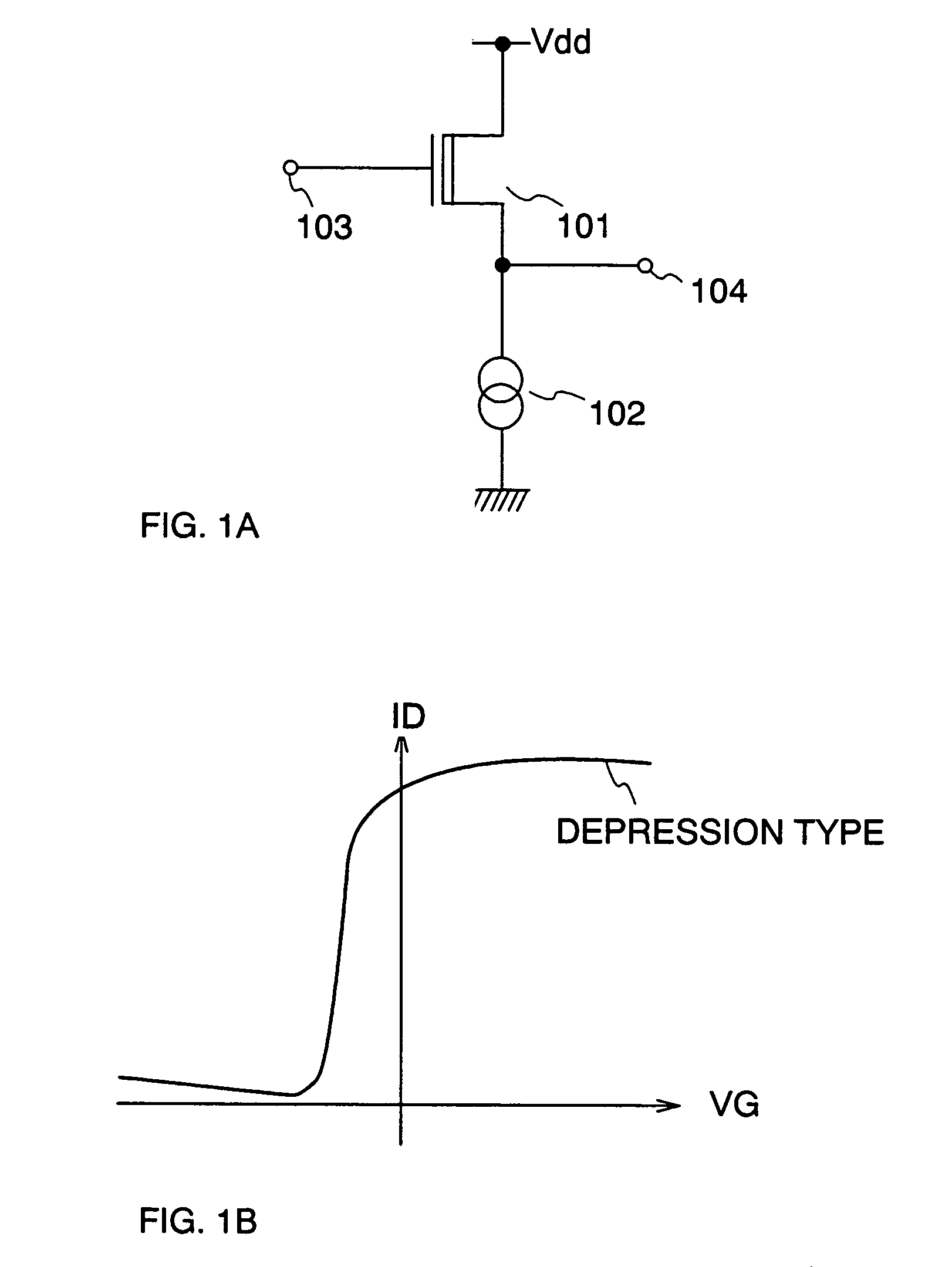
[0040]FIG. 1A shows a source follower circuit having a depletion mode TFT 101 of the invention, a constant current source 102, an input terminal 103, and an output terminal 104. Further, the depletion mode TFT 101 is connected to a power supply line Vdd. Note that the depletion mode TFT in the drawings of the invention is described by using a symbol as the depletion mode TFT 101.

[0041]Further, FIG. 1B shows a VG-ID characteristics of the depletion mode TFT. It is found when compared with FIG. 5B that a voltage (VGS) between the gate and source of the depletion mode TFT is quite small. That is, the voltage (VGS) between the gate and source of the depletion mode TFT is approximately 0 to 1 V; therefore, there is no need to increase an input voltage as described above.

[0042]Furthermore, the constant current source 102 may employ a known technique. In the case of using a polycrystalline silic...

embodiment mode 2

[0047]In this embodiment mode, a bootstrap circuit using a depletion mode TFT is described.

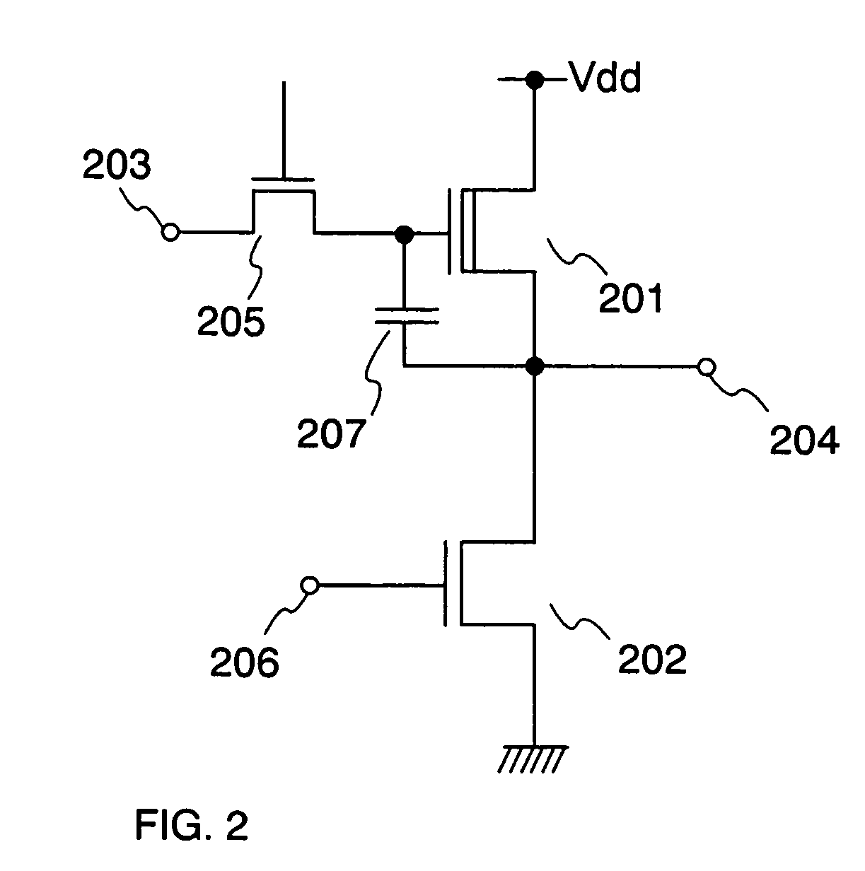
[0048]FIG. 2 shows a bootstrap circuit having an n-channel depletion mode TFT 201, a TFT 205, an n-channel enhancement mode TFT 202, an input terminal 203, an output terminal 204, an input terminal 206, and a capacitor 207. The depletion mode TFT is connected to a power supply line Vdd.

[0049]A bootstrap circuit is operated with the gate voltage of a TFT connected to a power supply line increased to be equal to or more than Vdd; however, it is difficult to actually increase a power source sufficiently due to a parasitic capacitance or the like. However, the depletion mode TFT 201 of the invention does not require as large gate voltage as an enhancement mode TFT. As described above, the depletion mode TFT has a characteristic that the threshold voltage is on its negative voltage side and a voltage (VGS) between the gate and source is approximately 0 V, while a voltage (VGS) between the gate and ...

embodiment mode 3

[0051]A signal driver circuit using the source follower circuit of the invention is described in this embodiment mode.

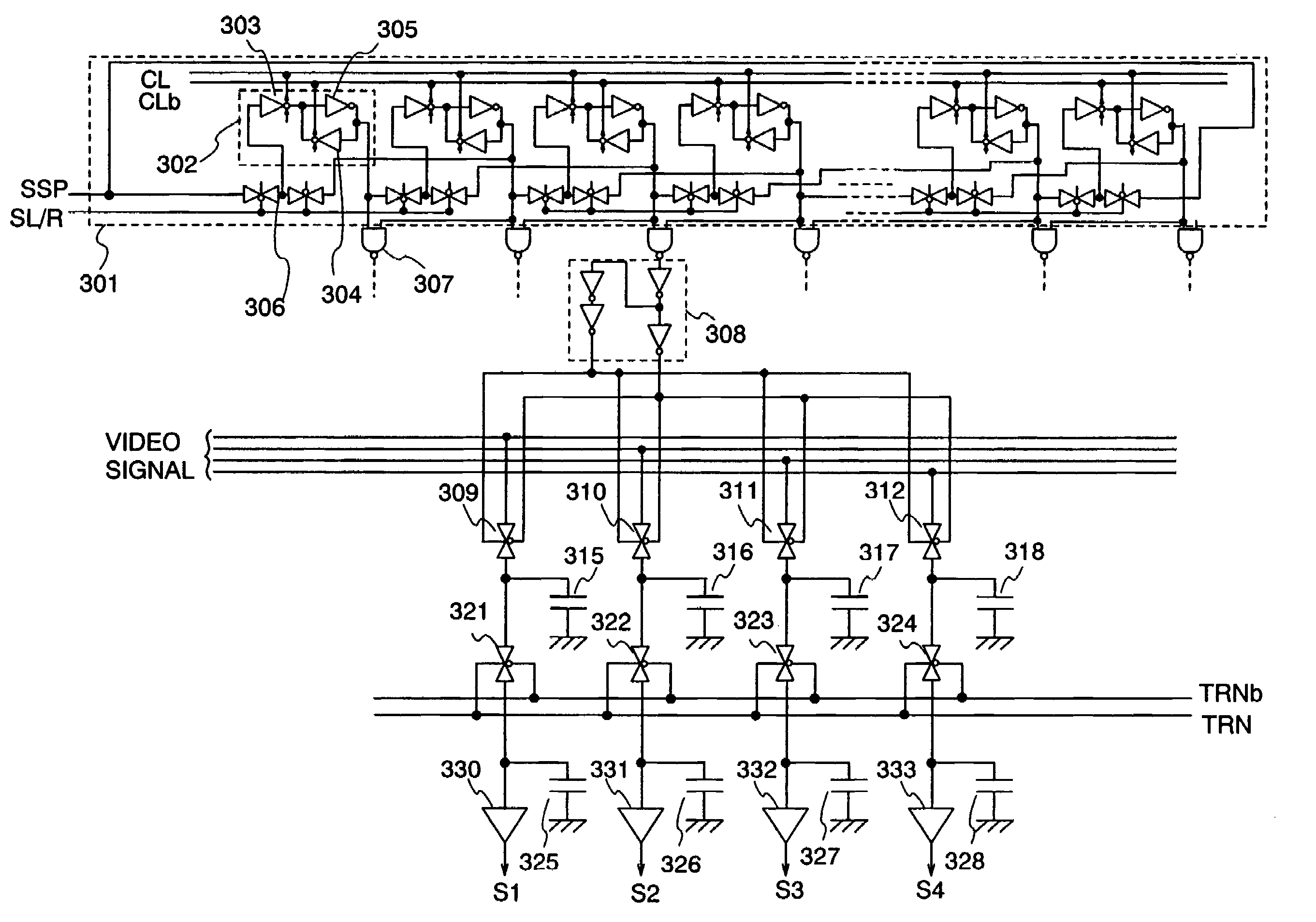
[0052]FIG. 3 shows a signal driver circuit having a shift register 301, a NAND circuit 307, and a buffer circuit 308.

[0053]First, a source start pulse SSP is inputted to a first stage of the shift register 301 through a switch 306. The switch 306 defines the scanning direction of the shift register 301. When a scanning direction switching signal SL / R is Lo, scanning is performed from left to right in FIG. 3, and right to left when the signal is Hi. Each stage of the shift register 301 is configured with a DFF (delay flip flop) 302 having clocked inverters 303 and 304 and an inverter 305. A pulse is shifted by the inverters in accordance with an input of a clock pulse CL and CLb.

[0054]An output of the shift register 301 is inputted to the buffer circuit 308 through the NAND circuit 307. Analog switches 309 to 312 are turned ON by an output of the buffer circuit 308, a...


PUM

PropertyMeasurementUnit
sizeaaaaaaaaaa
voltageaaaaaaaaaa
voltageaaaaaaaaaa

Abstract

In the case of using an analog buffer circuit, an input voltage is required to be added a voltage equal to a voltage between the gate and source of a polycrystalline silicon TFT; therefore, a power supply voltage is increased, thus a power consumption is increased with heat. In view of the foregoing problem, the invention provides a depletion mode polycrystalline silicon TFT as a polycrystalline silicon TFT used in an analog buffer circuit such as a source follower circuit. The depletion mode polycrystalline silicon TFT has a threshold voltage on its negative voltage side; therefore, an input voltage does not have to be increased as described above. As a result, a power supply voltage requires no increase, thus a low power consumption of a liquid crystal display device in particular can be realized.

Description

BACKGROUND OF THE INVENTION[0001]1. Field of the Invention[0002]The present invention relates to an analog buffer circuit such as a source follower circuit using a polycrystalline thin film transistor. The invention also relates to a signal driver circuit and an active matrix liquid crystal display device having the source follower circuit of the invention.[0003]2. Description of the Related Art[0004]Recently, a technology regarding a semiconductor device formed on an insulating substrate by using a thin film transistor (hereinafter referred to as a TFT) is rapidly developed. Further, as for a semiconductor device having a polycrystalline semiconductor film by making an amorphous semiconductor film into a polycrystalline semiconductor film by heating or laser irradiation, a pixel portion and a driver circuit can be integrated; therefore, miniaturization and realization of a narrower frame (to increase the ratio of the pixel portion to the display portion) of a semiconductor device a...

Claims


Application Information

Patent Timeline
Patent Type & Authority Patents(United States)
IPC IPC(8): H01L27/12G02F1/1368G09G3/20G09G3/36H01L27/08H01L29/786H03F1/02H03F1/22H03F3/50
CPCG09G3/3688H03F1/223H03F3/505H03F1/02G09G3/2074G09G2330/021H01L29/78672H03F2200/513H03F2200/51
Inventor KOYAMA, JUN
Owner SEMICON ENERGY LAB CO LTD
Why Eureka
Try Eureka