Apparatus and Method for High Voltage Bandgap Type Reference Circuit with Flexible Output Setting
- Summary
- Abstract
- Description
- Claims
- Application Information
AI Technical Summary
Benefits of technology
Problems solved by technology
Method used
Image
Examples
first embodiment
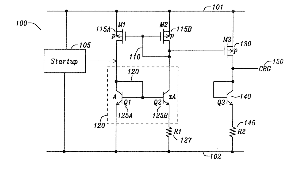
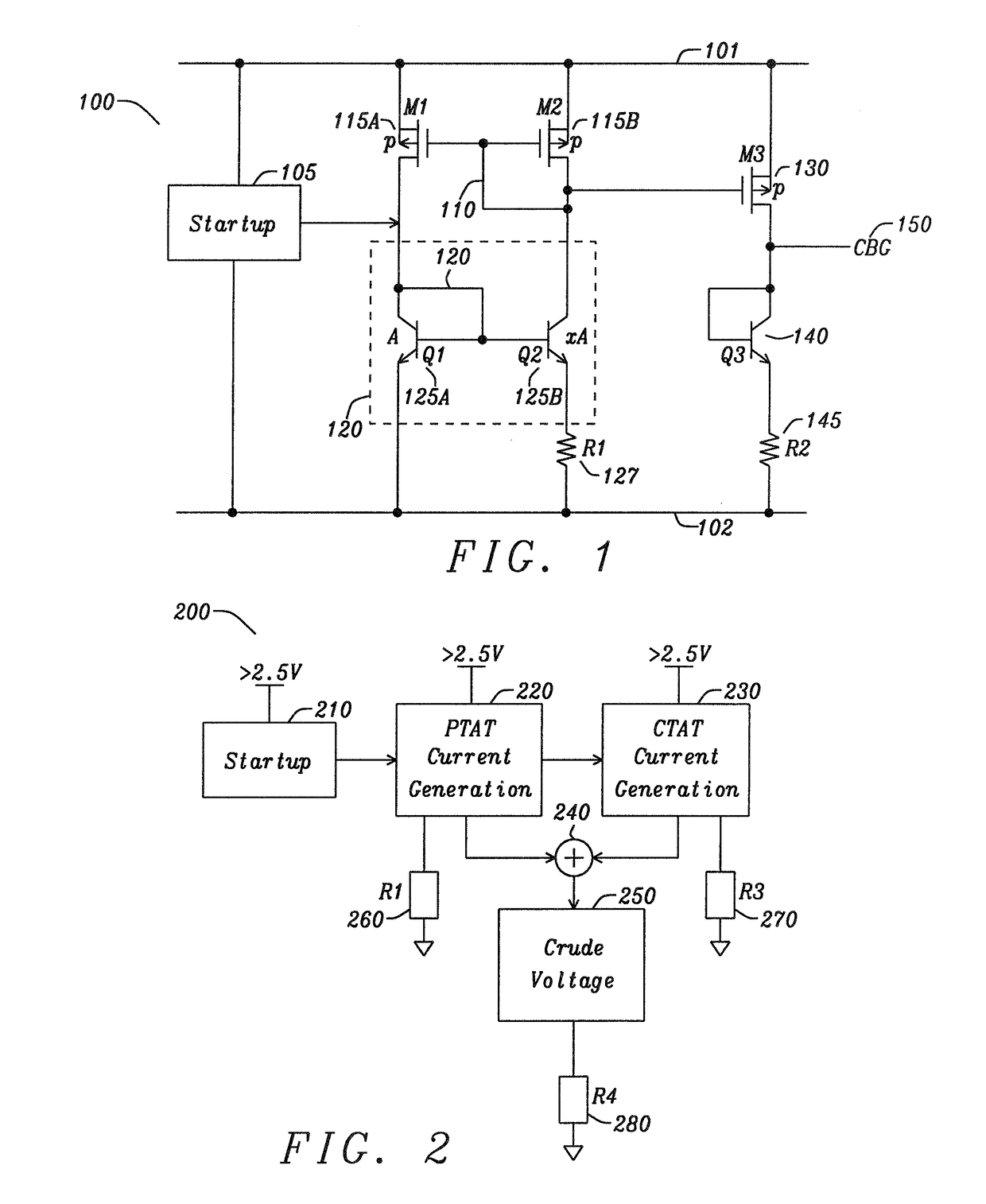
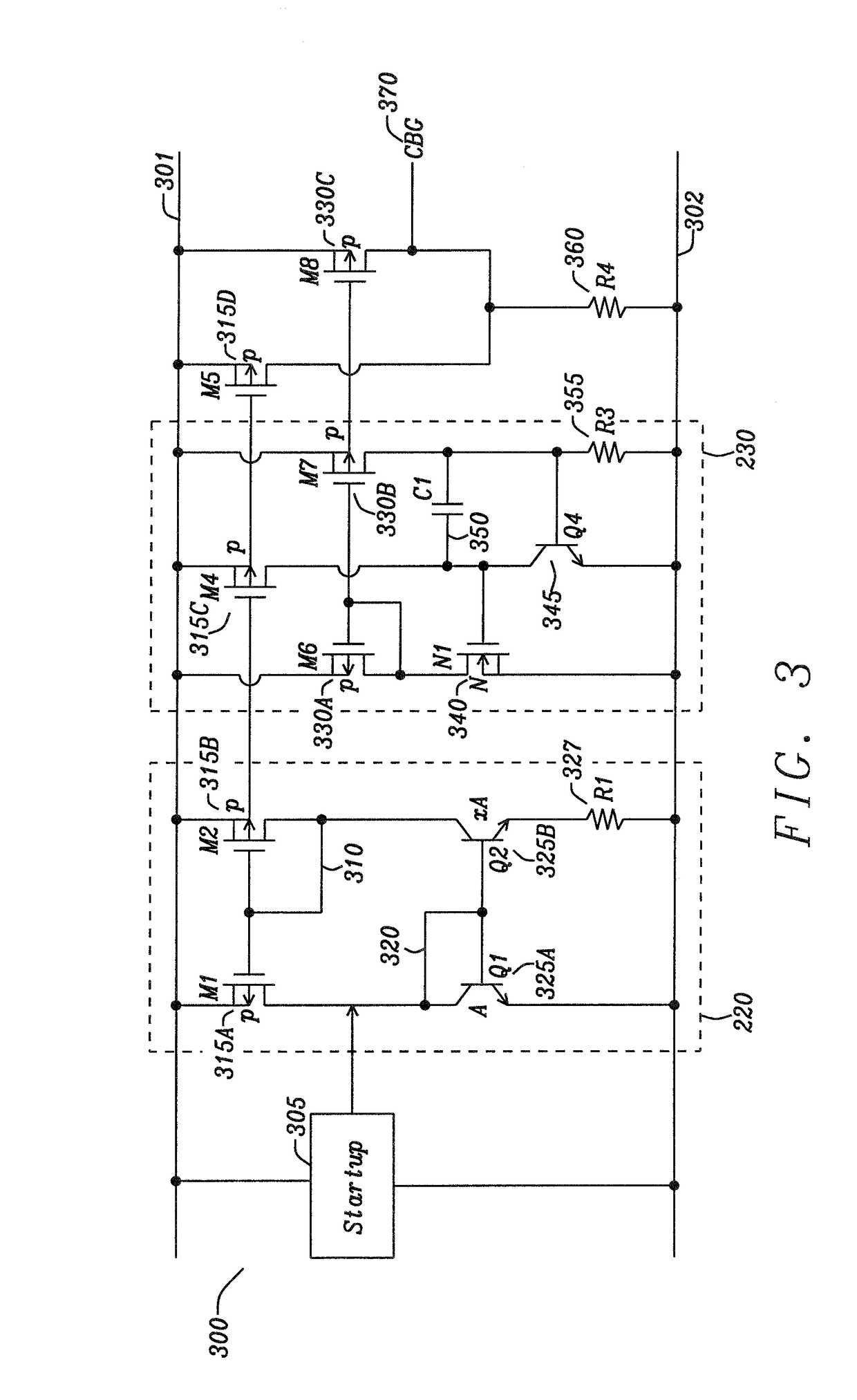
[0045]FIG. 2 is a high-level circuit schematic of a voltage reference circuit in accordance with the disclosure. FIG. 2 illustrates the circuit 200 of a voltage reference network comprises a startup block 210, a PTAT Current Generation block 220, a CTAT Current Generation block 230, an adder block 240, and a reference voltage block 250. A crude reference voltage 250 using PTAT and CTAT currents are summed such that their temperature coefficients compensate each other. The sum of the PTAT and CTAT currents is constant with respect to temperature. Over a wide temperature range, the behavior of this circuit is stable enough to adequately supply reference voltage levels to the other circuits. Therefore, additional circuitry is required to generate the desired reference voltages that are different from this reference voltage. Resistor R1260 is coupled to the PTAT Current Generation block 220. Resistor R3270 is coupled to CTAT Current Generation block 230. Resistor R4280 is coupled to the...
second embodiment
[0047]FIG. 4 is a circuit schematic of a voltage reference circuit in accordance with the disclosure. The voltage reference 400 operates at higher supply voltages by further utilization of protection elements high voltage n-channel (HN) transistors and high voltage p-channel (HP) transistors. The circuit 400 comprises a power supply rail VDD 401, and ground VSS rail 402. The circuit 400 comprises a PTAT Current Generator 403, a CTAT Current Generator 404, and startup circuit 405 blocks. The startup circuit 405 couples into the PTAT generation circuit. The PTAT Current Generator comprises npn bipolar junction transistor (BJT) current mirror 420 with transistor Q1425A of size A and transistor 425B of size xA. The current mirror 420 is coupled to resistor R1427. A high voltage stage forming a current mirror comprises of a p-channel MOSFET HN1429A and HN2429B. A second high voltage stage forming a current mirror of a p-channel MOSFET HP1417A and 417B. This current mirror formed by 417A ...
embodiment 640
[0055]FIG. 6 is a comparison of transient voltage simulation 600 of a prior art voltage reference circuit 620 and a bandgap voltage reference circuit 640 in accordance with an embodiment of the disclosure. In FIG. 6, it can be seen that the disclosed embodiment 640 quickly provides the reference voltage, and more importantly more smoothly and accurately for all corner cases. This provides faster settling for the rest of the circuit. The embodiment of the disclosure response 640 settles much more smoothly avoiding glitches and other possible problems. Also the steady state values of the reference voltage have much less variation over corners. The circuit provides lower variation once the circuit reaches a steady state, which is evident from the smaller spread in the lower curves as compared to the upper curves. Additionally, the startup curves are smoother.
[0056]FIG. 7 is an expanded view comparison of bandgap output voltage simulation 800 of a bandgap output voltage of a prior art v...
PUM
 Abstract
Description
Claims
Application Information


