Semiconductor device and display device

a semiconductor and display device technology, applied in semiconductor devices, digital storage, instruments, etc., can solve the problems of low power use efficiency of power supply circuits, impede the reduction in size and weight of display devices, and extremely high power consumption of circuits formed using tft of low temperature polysilicon, and achieve the effect of low power consumption

Inactive Publication Date: 2014-08-12
SEMICON ENERGY LAB CO LTD
View PDF70 Cites 19 Cited by
  • Summary
  • Abstract
  • Description
  • Claims
  • Application Information

AI Technical Summary

Benefits of technology

[0005]However, there has been a problem in that a circuit formed using a TFT of low temperature polysilicon has extremely high power consumption because power supply voltage is high or signal amplitude is large. In addition, in order to operate the circuit formed using the TFT of low temperature polysilicon, it has been necessary to increase the power supply voltage. Therefore, it has been necessary to supply power supply voltage dedicated for the circuit formed using the TFT of low temperature polysilicon Since the size of a module of a power supply circuit which supplies the dedicated power supply voltage is large, the power supply circuit has impeded reduction in size and weight of a display device. Further, the power supply circuit has had low power use efficiency. Therefore, wasted power has been increased, so that power consumption has been increased.

Problems solved by technology

However, there has been a problem in that a circuit formed using a TFT of low temperature polysilicon has extremely high power consumption because power supply voltage is high or signal amplitude is large.
Therefore, it has been necessary to supply power supply voltage dedicated for the circuit formed using the TFT of low temperature polysilicon Since the size of a module of a power supply circuit which supplies the dedicated power supply voltage is large, the power supply circuit has impeded reduction in size and weight of a display device.
Further, the power supply circuit has had low power use efficiency.
Therefore, wasted power has been increased, so that power consumption has been increased.

Method used


Image

  • Semiconductor device and display device
  • Semiconductor device and display device
  • Semiconductor device and display device

Examples


embodiment mode 1

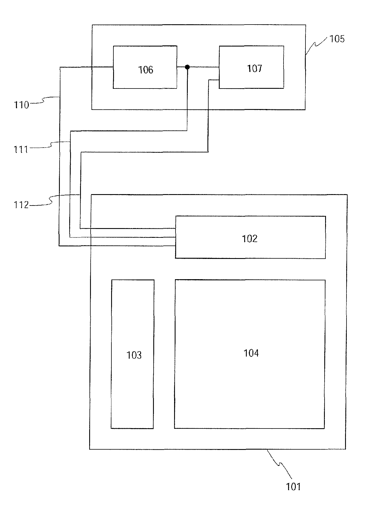
[0134]As shown in FIG. 1, a glass substrate 101 is provided with a source driver 102 and a gate driver 103 as driver circuits which drive pixels, and pixel arrangement 104. Note that the present invention is not limited to this, and the glass substrate 101 can be provided with various circuits. All or part of these circuits are / is formed using a TFT which is formed over an insulating substrate by extracting a single-crystal semiconductor layer from a single-crystal semiconductor substrate and fixing the single-crystal semiconductor layer to the insulating substrate, or a TFT winch is formed over an insulating substrate by attaching a single-crystal semiconductor substrate to the insulating substrate and fixing a single-crystal semiconductor layer which is part of the single-crystal semiconductor substrate to the insulating substrate by separating the single-crystal semiconductor substrate. Note that a TFT which is formed over an insulating substrate by extracting a single-crystal se...

embodiment mode 2

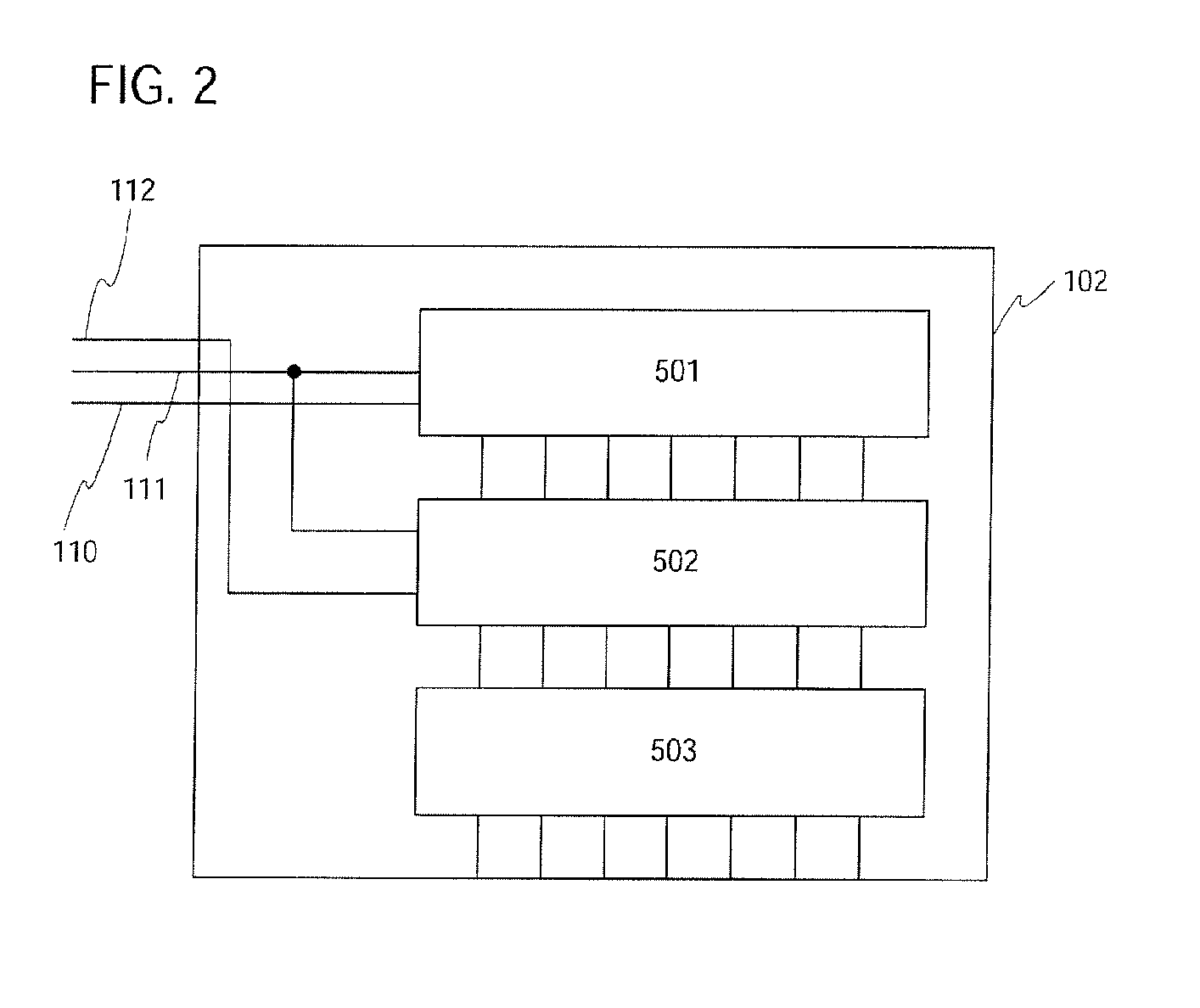
[0167]In tins embodiment mode, a specific example of the structure described in Embodiment Mode 1 is described. FIG. 9A shows an example of a shift register. The shift register includes a clocked inverter 801, an inverter 802, a NAND circuit 803, and the like. A signal transmitted from the controller 106 is input to the shift register through a wiring 800. Then, the signal is output from a wiring 804 through the clocked inverter 801, the inverter 802, the NAND circuit 803, and the like. Note that a clock signal (CLK) and a clock inverted signal (CLKB) are input to the clocked inverter 801. Each of the first latch circuit 601 and the second latch circuit 602 in FIG. 3 also includes a clocked inverter, an inverter, and the like and has a circuit structure which is similar to that in FIG. 9A.

[0168]FIG. 9B shows an example of the clocked inverter 801 which is used in the shift register. The clocked inverter 801 includes a first P-channel transistor 809, a second P-channel transistor 810...

embodiment mode 3

[0183]Next, a method for manufacturing a single-crystal TFT is described.

[0184]FIGS. 18A and 18B each show an SOI substrate. In FIG. 18A, a base substrate 2100 is a substrate having an insulating surface or an insulating substrate, and any of various glass substrates which are used in the electronics industry, such as aluminosilicate glass substrates, aluminoborosilicate glass substrates, and barium borosilicate glass substrates can be used. Alternatively, a quartz glass substrate or a semiconductor substrate such as a silicon wafer can be used. An SOI layer 2102 is a single-crystal semiconductor, and single-crystal silicon is typically used. Alternatively, a single-crystal semiconductor layer formed of silicon, germanium, or a compound semiconductor such as gallium arsenide or indium phosphide which can be separated from a single-crystal semiconductor substrate by a separation method of hydrogen ion implantation can be used.

[0185]Between the base substrate 2100 and the SOI layer 21...


PUM

PropertyMeasurementUnit
voltageaaaaaaaaaa
voltageaaaaaaaaaa
thicknessaaaaaaaaaa

Abstract

A single-crystal semiconductor layer is separated from a single-crystal semiconductor substrate and is fixed to an insulating substrate to form a TFT over the insulating substrate. Then, a driver circuit is formed using the TFT. The TFT has excellent current characteristics because an active layer is almost in a single-crystal state. Accordingly, a small thin display device with low power consumption can be manufactured. Further, a controller and a shift register which is included in a source driver are operated at the same power supply voltage. Thus, power consumption can be reduced.

Description

BACKGROUND OF THE INVENTION[0001]1. Field of the Invention[0002]The present invention relates to an object, a method, or a method for producing an object. In particular, the present invention relates to a display device or a semiconductor device. Specifically, the present invention relates to a display device in which a single-crystal semiconductor is fixed to an insulating substrate.[0003]2. Description of the Related Art[0004]In recent years, a display device in which not only a pixel but also a driver circuit is formed over a glass substrate has been developed. As a pixel, a liquid crystal element, an organic EL element, or the like is used. At this time, a circuit is formed over a glass substrate by using a thin film transistor (TFT) formed of low temperature polysilicon. However, the TFT has worse current characteristics and higher threshold voltage than those of a transistor formed of a single crystal. Therefore, operations are performed with power supply voltage or signal amp...

Claims


Application Information

Patent Timeline
Patent Type & Authority Patents(United States)
IPC IPC(8): G09G3/36G02F1/1345H01L29/66H01L27/12
CPCH01L29/66772G09G3/3648G02F1/13454G09G2300/0408H01L27/1218G09G2330/021H01L27/1214H01L27/12G11C19/30G11C19/28
Inventor KIMURA, HAJIMEUMEZAKI, ATSUSHI
Owner SEMICON ENERGY LAB CO LTD
Why Eureka
Try Eureka