Group-III nitride light-emitting device

a light-emitting device and nitride technology, applied in the direction of solid-state devices, lasers, semiconductor lasers, etc., can solve the problems of difficult growth of the ingan well layer, significant blue shift of wavelength along with current injection, and inability to achieve the effect of improving the quantum efficiency, so as to improve the quantum efficiency of the light-emitting device, improve the crystal quality of the barrier layer, and increase the incorporation of indium atoms into the well layer

Active Publication Date: 2011-06-28
SUMITOMO ELECTRIC IND LTD
View PDF22 Cites 238 Cited by
  • Summary
  • Abstract
  • Description
  • Claims
  • Application Information

AI Technical Summary

Benefits of technology

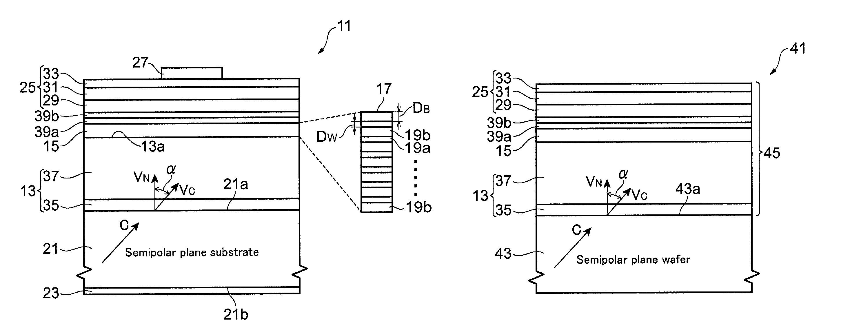
[0017]The film thickness of the well layer of the active layer formed on the semipolar plane inclined at the above-described inclination angle is 4 nm or more, and 10 nm or less and, therefore, is larger than the thickness of the well layer of the active layer formed on a c-plane. In this case, the piezoelectric field is reduced and, thereby, a significant blue shift of wavelength and a reduction in quantum efficiency along with an increase in current are reduced.
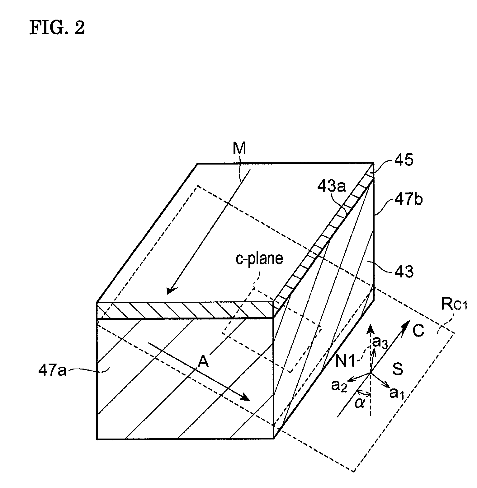
[0044]In the method according to an embodiment of the present invention, the above-described inclination angle may be specified in an m-axis direction of InSAlTGa1-S-TN of the above-described substrate, and the off-angle of the above-described inclination angle may be within the range of −1 degree or more, and +1 degree or less with reference to an a-axis. According to this method, control of the direction in which the inclination angle is specified becomes easy.

Problems solved by technology

Consequently, an effect of improving the quantum efficiency is not obtained, and a blue shift of wavelength along with current injection becomes significant.
If the inclination angle exceeds 85 degrees, growth of the InGaN well layer becomes difficult.
Since the piezoelectric field is suppressed with respect to the semipolar plane, an increase in wavelength due to band bending of the quantum well active layer cannot be expected.
As a result, the crystal quality of the InGaN well layer is degraded, and the emission characteristics deteriorate.
If the thickness of the InGaN well layer exceeds 10 nm, the crystal quality is degraded and the emission characteristics deteriorate.

Method used


Image

  • Group-III nitride light-emitting device
  • Group-III nitride light-emitting device
  • Group-III nitride light-emitting device

Examples


example 1

[0086]A flow 100a of key steps for producing a light-emitting device will be described with reference to FIG. 4. In Step S101, a GaN wafer was prepared. The resulting GaN wafer exhibited n-type conductivity and had a basal plane inclined at an inclination angle of 25 degrees from a c-plane in the direction of an m-axis. The GaN wafer was produced as described below. A 2-inch-size GaAs wafer was prepared. A stripe-shaped insulating mask composed of a silicon oxide was formed on the GaAs wafer having a (111) plane which was 25 degrees off in a (100) direction. Thereafter, a GaN thick film was grown on the resulting wafer by an HVPE method. The GaN thick film included low-defect-density regions and high-defect-density regions arranged alternately. Each of the low-defect-density regions and high-defect-density regions took on the shape of a stripe. Threading dislocation in the low-defect-density region extended in the direction of the c-axis, and the threading dislocation density thereo...

example 2

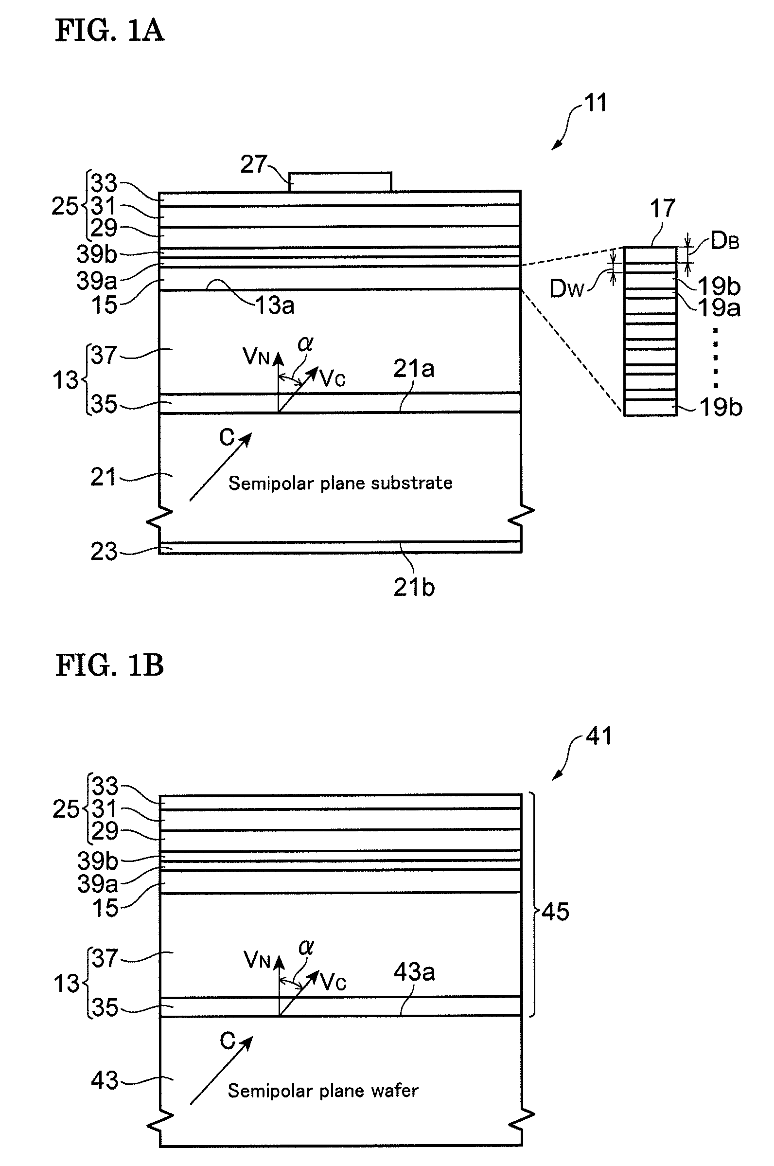
[0097]Key steps for producing the light-emitting device will be described again with reference to FIG. 4. In the manufacturing method of the present example, Step S109 is conducted after Step S103 prior to Step S104.

[0098]In Step S109, an In0.02Ga0.98N layer was grown on the n-type GaN layer. In Step S104, the quantum well structure including 3 well layers was formed on the In0.02Ga0.98N layer. The well layer and the barrier layer of the active layer had the thicknesses of 5 nm and 15 nm, respectively. Subsequently, a p-type GaN based semiconductor region was grown by using the same steps as in Example 1, so that an epitaxial wafer including an LED epitaxial structure was produced.

[0099]The resulting epitaxial wafer was taken out of the reactor. In Step S108, a translucent p-side electrode 400 μm square was formed on the p-type GaN layer of the epitaxial wafer and, in addition, an n-side electrode was formed on the back surface of the GaN wafer so as to produce a substrate product. ...

example 3

[0101]Key step for producing a laser diode device will be described with reference to FIG. 6. A GaN wafer produced as in Example 1 was prepared. The resulting GaN wafer had a basal plane inclined at an inclination angle of 25 degrees from a c-plane in the direction of an a-axis. The GaN wafer included low-defect-density regions and high-defect-density regions arranged alternately. Each of the low-defect-density regions and high-defect-density regions took on the shape of a stripe. Threading dislocations in the low-defect-density region extended in the direction of the c-axis, and the threading dislocation density thereof was less than 1×106 cm−2 in the c-plane. A laser diode device was produced on the GaN wafer by an organic metal chemical vapor deposition method on the basis of the procedure described below. In Step S102, the GaN wafer was placed on a susceptor in a growth reactor, was suspended once, and the substrate temperature was changed to 870° C. Thereafter, nitrogen was ser...


PUM


Abstract

A group-III nitride light-emitting device is provided. An active layer having a quantum well structure is grown on a basal plane of a gallium nitride based semiconductor region. The quantum well structure is formed in such a way as to have an emission peak wavelength of 410 nm or more. The thickness of a well layer is 4 nm or more, and 10 nm or less. The well layer is composed of InXGa1-XN (0.15≦X<1, where X is a strained composition). The basal plane of the gallium nitride based semiconductor region is inclined at an inclination angle within the range of 15 degrees or more, and 85 degrees or less with reference to a {0001} plane or a {000-1} plane of a hexagonal system group III nitride. The basal plane in this range is a semipolar plane.

Description

BACKGROUND OF THE INVENTION[0001]1. Field of the Invention[0002]The present invention relates to a group-III nitride light-emitting device and a method for manufacturing a group-III nitride based semiconductor light-emitting device.[0003]2. Description of the Related Art[0004]Japanese Journal of Applied Physics Vol. 45, No. 26, 2006, pp. L659-L662 (Non-Patent Document 1) describes InGaN light-emitting diodes. These light-emitting diodes were produced on a semipolar (11-22) plane (58 degrees off the c-plane in an a-axis direction) GaN substrates. The light-emitting diodes had single quantum well structures composed of an InGaN well layers having a width of 3 nm. The following characteristics were attained. Regarding blue emission (wavelength 430 nm), the optical output was 1.76 mW, and the external quantum efficiency was 3.0%. Regarding green emission (wavelength 530 nm), the optical output was 1.91 mW, and the external quantum efficiency was 4.1%. Regarding amber emission (wavelengt...

Claims


Application Information

Patent Timeline
Patent Type & Authority Patents(United States)
IPC IPC(8): H01L29/74H01L31/111B82Y20/00H01L33/06H01L33/32
CPCB82Y20/00H01L33/06H01L33/16H01L21/02389H01L21/02433H01L21/02458H01S5/34333H01L21/0262H01L33/32H01L21/0254
Inventor AKITA, KATSUSHIKASAI, HITOSHIKYONO, TAKASHIMOTOKI, KENSAKU
Owner SUMITOMO ELECTRIC IND LTD
Why Eureka
Try Eureka