Bi-directional signal transmission system

a transmission system and bi-directional technology, applied in the direction of logic circuits, logic circuit coupling/interface arrangements, electrical devices, etc., can solve the problems of affecting the i2c function of the bus, the maximum possible speed of the bus, and the possibility of oscillation in such a loop

Active Publication Date: 2008-08-26
INTEGRATED ELECTRONICS SOLUTIONS
View PDF3 Cites 16 Cited by
  • Summary
  • Abstract
  • Description
  • Claims
  • Application Information

AI Technical Summary

Problems solved by technology

If the bus capacitance is increased then the maximum possible speed of the bus is limited, and the slower rise times on the bus start to cause difficulties.
Most of these circuits have problems which may be associated with latching, be only conditionally stable, or present glitches.
The usual limitation presented by such circuits is that they are unable to reverse their direction of signal flow when active, generating a glitch that can upset the bus I2C function.
Oscillation in such a loop becomes another possible problem.
A more subtle problem arises because the I2C Bus protocol has been defined so that two or more ICs are permitted to transmit (that is pull the I2C bus low) at the same time.
Most of the circuits that have been suggested as providing a suitable buffering action have a problem that arises during this bus contention function.
They fail to buffer the signals in a manner that does not generate spurious signals.
However in all of the published circuits there is a delay between the time the active forward path switches off, and the reverse path is activated.
Unfortunately many proposed circuits fail this glitch test, and allow the input to go high for the time needed for the buffer circuit to recognise that the direction of the signal path has reversed.

Method used


Image

  • Bi-directional signal transmission system
  • Bi-directional signal transmission system
  • Bi-directional signal transmission system

Examples


Embodiment Construction

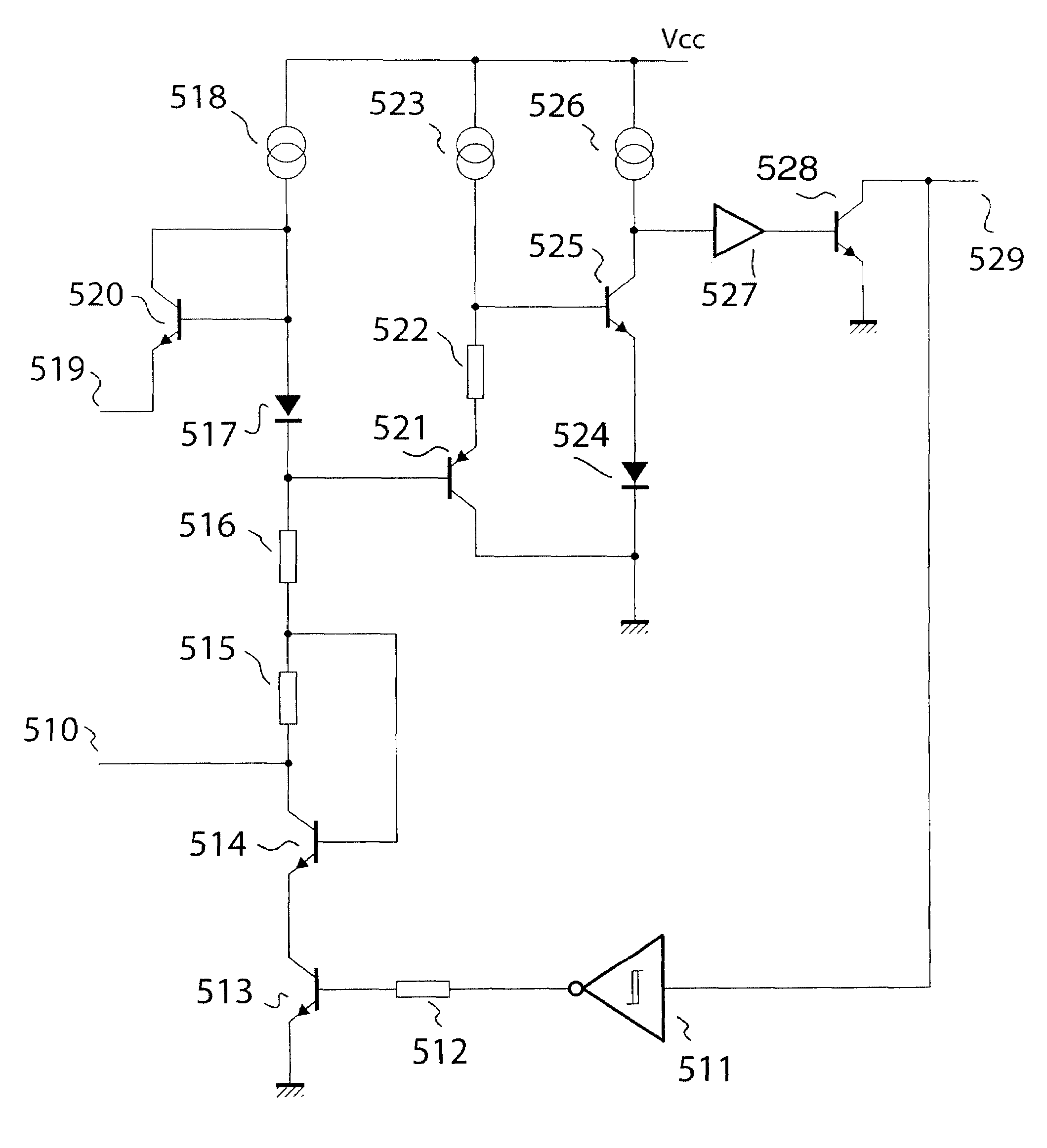
[0032]FIG. 1 shows the structure of the OM1896 buffer as described in U.S. Pat. No. 6,014,040. In this circuit the OM1896 integrated circuit 101 contains two identical buffers. The input connected to the first bi-directional signal path 111 is normally pulled high by the pull-up mechanism on that signal path. When it is high the input voltage is more positive than the reference voltage Vref on the comparator 114. This puts a low level on the base of transistor 115, and the output connected to the second bi-directional signal path 112 is able to be pulled high by the pull-up mechanism on that path.

[0033]With temperature the medium reference voltage Vref is designed to follow the low voltage generated by a low logic signal on the reverse input 113, and in the OM1896 is normally made up of a transistor circuit based on a single transistor emitter base voltage reduced by an offset voltage component generated by the voltage drop derived from the voltage across an integrated resistor carr...


PUM


Abstract

A bi-directional signal transmission system including, a first bi-directional signal path having circuitry adapted to generate a logic high level on said first path, one or more first stations connected to the first bi-directional signal path adapted to monitor a logic level on said first path, and to generate a logic low level on said first path, an interface device operatively coupled to the first bi-directional signal path, said interface device having a first receive input also capable of functioning as an output capable of pulling the first path low; and a second bi-directional signal path coupled to a transmit output and a receive input on the buffered side of the interface device, said interface device includes a first means for generating on the first bi-directional signal path a medium logic level in response to a low level on the receive input on the buffered side, and a second means for generating on the transmit output on the buffered side, a low logic level in response to a low level on the first bi-directional signal path, otherwise generating a high level on the said transmit output, wherein the one or more first stations are adapted to detect the medium and the low levels on the first bi-directional signal path as LOW, and the high logic level on the first bi-directional signal path as HIGH, and wherein further the first means for generating the medium logic level on the first signal path includes an open collector transistor, the emitter of which is connected to VEE, with its collector pulling the first signal path low through a diode connected transistor.

Description

TECHNICAL FIELD[0001]This invention relates to a bi-directional signal transmission system for transmission of a binary signal in both directions. It further relates to improvements in providing a buffered interface in such a system.BACKGROUND ART[0002]A number of two wire bi-directional signal transmission systems have been extensively used. One such system is the Integrated Circuit Bus system (I2C Bus system), disclosed in the Philips Data Handbook IC12a, 1989, and “The I2C Bus and how to use it (including specifications)” 1995 Philips Semiconductors.[0003]The I2C Bus system is a serial bus system between individual integrated circuits, or stations, that are interconnected through a bidirectional two wire transmission channel. Of the two wires, one carries a clock signal, and the other the data, with a predetermined communication protocol. Depending on the particular function within the system, an individual station can act as the transmitter, or as a receiver, or both.[0004]The I...

Claims


Application Information

Patent Timeline
Patent Type & Authority Patents(United States)
IPC IPC(8): H03K19/0175
CPCH03K19/0826H03K19/01843
Inventor CRAWFORD, JOHN
Owner INTEGRATED ELECTRONICS SOLUTIONS
Why Eureka
Try Eureka