Stamper for molding article and method of producing said stamper

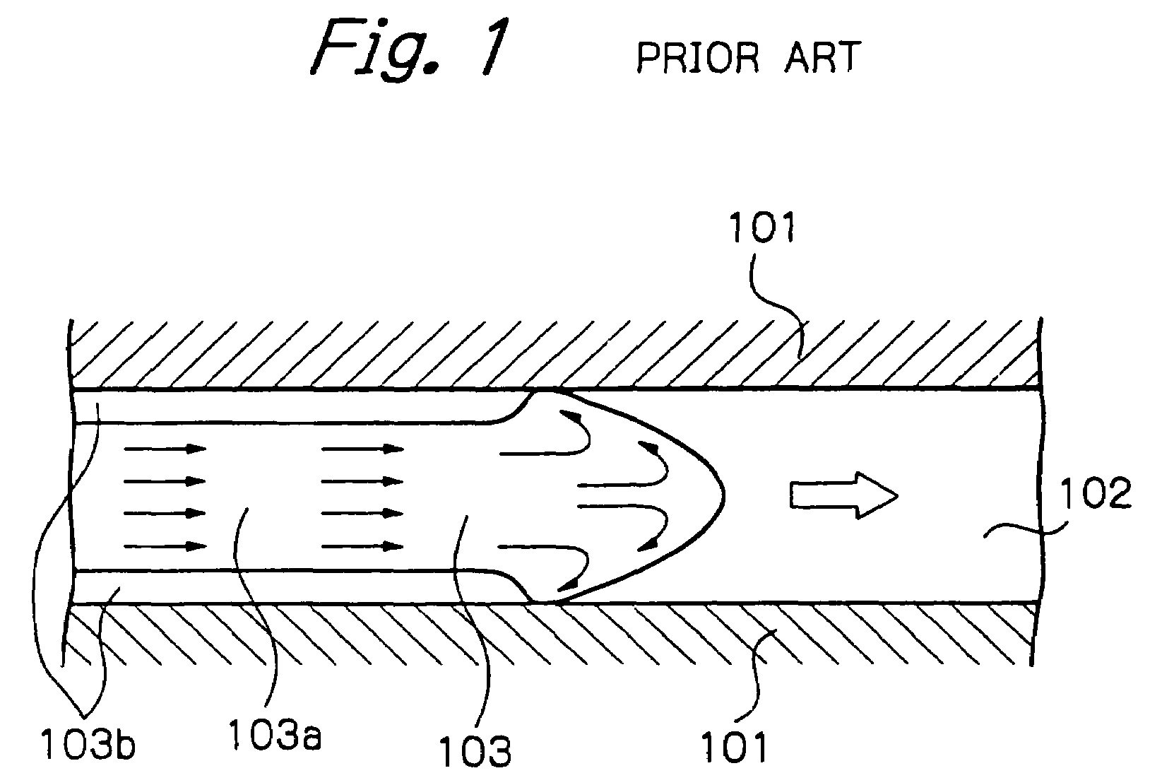
a technology of stamping stamping and molding article, which is applied in the field of optical disk, can solve the problems of reducing the yield of optical disks, reducing the transferability of optical disks, and none of the above conventional technologies can enhance the transferability and tact of a disk base molding cycle at a high level, so as to enhance both the transferability and the tact of a disk base molding cycl

Inactive Publication Date: 2008-09-02
RICOH KK
View PDF24 Cites 7 Cited by
  • Summary
  • Abstract
  • Description
  • Claims
  • Application Information

AI Technical Summary

Benefits of technology

[0011]It is therefore an object of the present invention to enhance both the transferability and the tact of a disk base molding cycle at the same time.
[0014]It is a further object of the present invention to provide an optical disk sufficiently compatible with commercially available CD players by allowing guide grooves filled with a pigment by spin coating to have a substantially uniform configuration at any position in the radial direction.

Problems solved by technology

Specifically, the mold temperature should be as low as possible for increasing the tact, but would degrade transferability if excessively low.
On the other hand, a high mold temperature would enhance transferability, but would increase a period of time necessary for the resin to be cooled to a parting temperature and would thereby lower the yield of optical disks.
However, none of the above conventional technologies can enhance both the transferability and the tact of a disk base molding cycle at a high level.
Laid-Open Publication No. 6-259815 has a problem that the Ni film formed on the transfer surface of a stamper obstructs the fine patterning of the-transfer surface.
Laid-Open Publication No. 10-149587 has a problem that the mold itself must be redesigned or replaced, wasting existing molding equipment.
While the thickness distribution of the recording layer can be controlled on the basis of coating conditions, it is difficult to control the distribution of the pigment in guide grooves.
This scatters reflectance and tracking error and other signal characteristics and makes it difficult to produce constant quality, reliable optical disks.
In addition, the resulting optical disks are not satisfactorily compatible with commercially available CD players.
None of such implementations, however, gives consideration to the decrease in the fluidity of molten resin ascribable to temperature fall.
Therefore, the implementations cannot realize desirable transferability alone when a high cycle is desired, aggravating the scattering of optical disks in signal characteristics.

Method used


Image

  • Stamper for molding article and method of producing said stamper
  • Stamper for molding article and method of producing said stamper
  • Stamper for molding article and method of producing said stamper

Examples


1st embodiment

[0036]This embodiment pertains to the production of various kinds of optical disks including a CD, a CD-R, an MD (Mini Disk); an MO (Magnetooptical disk), PD (Phase change optical Disk) and a DVD (Digital Video Disk). In the following description, stampers are classified into a heat-insulated master stamper and a heat-insulated son stamper produced from a master by transfer via a mother. Both of these stampers are used to produce optical disk bases.

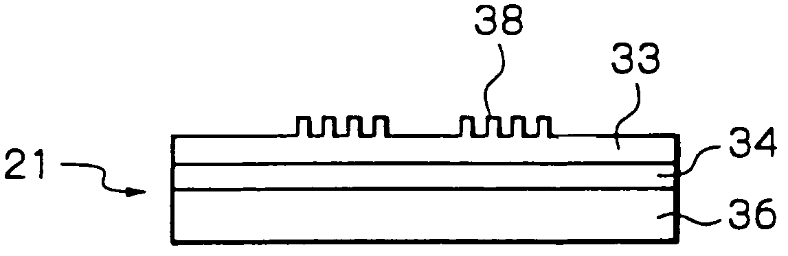
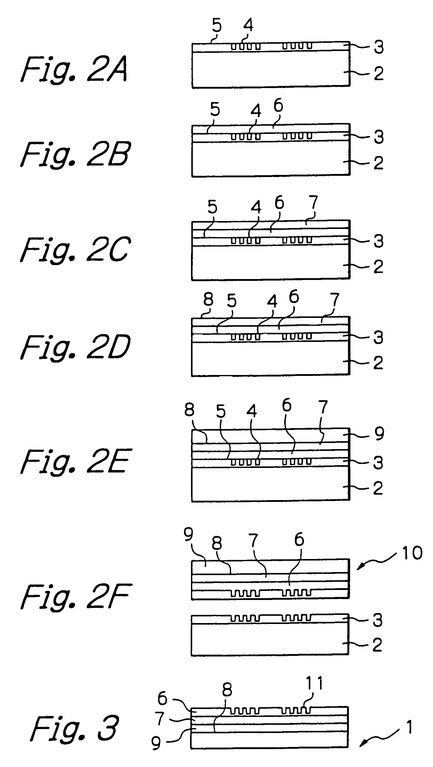
[0037]First, a heat-insulated master stamper and a method of producing it will be described with reference to FIGS. 2A-2F and FIG. 3. As shown in FIG. 2A, a photoresist layer 3 is formed on a glass master 2 and then exposed by a laser beam and developed to form a pattern of fine projections and recesses 4 constituting a disk surface pattern. The glass master 2 with the pattern 4 serves as a master. An electroconductive film layer 5 is formed on the pattern 4. Subsequently, as shown in FIG. 2B, Ni electroforming is effected by using the el...

2nd embodiment

[0088]Referring to FIGS. 10A through 10D, an alternative embodiment of the present invention that pertains to the product ion of a stamper will be described. First, how a mother 1 shown in FIG. 10A is formed before the sequence of steps shown in FIGS. 10A through 10D will be described. After an electroconductive film has been formed on a pattern of fine projections and recesses formed on a glass master, an Ni layer is formed by electroforming by using the electroconductive film as a cathode. Then, the glass master is separated to produce a master. After the master has been peeled off, an Ni layer is formed by electroforming and then separated from the master in order to produce the mother 1 having an inverted projection and recess pattern 1a.

[0089]After the mother 1 has been subjected to peeling and film forming like the master (not shown specifically), an about 25 μm thick Ni layer 2a is formed on the mother 1 by electroforming, as shown in FIG. 10A. In FIG. 10A, the reference num...

3rd embodiment

[0108]This embodiment is substantially identical with the first embodiment as to the heat-insulated stamper or son stamper, a method of producing it, an optical disk base, and a method of producing it. The following description will therefore concentrate on differences between this embodiment and the first embodiment.

[0109]As shown in FIG. 11, photoresist is applied to a glass master 2 such that its thickness sequentially increases from the inner circumference toward the outer circumference. Then, the photoresist is exposed to a guide groove pattern by a laser beam over a range of 22.35 mm to 59 mm from the center of the glass base 2. At this instant, as shown in FIG. 12, the relative intensity of the laser beam is sequentially increased from the inner-circumference toward the outer circumference of the glass master 2. After the exposure, the pattern was,developed to form guide grooves shown in FIG. 13A in the glass master 2. As shown, the guide grooves have depths sequentially incr...


PUM

PropertyMeasurementUnit
thicknessaaaaaaaaaa
thicknessaaaaaaaaaa
thicknessaaaaaaaaaa

Abstract

An optical disk and a method of producing it, particularly a stamper for molding a semiconductor disk base capable of forming an optical disk sufficiently compatible with commercially available CD (Compact Disk) players, a method of producing a stamper, a method of producing an optical disk base, a method of producing an optical disk, and an optical disk base and optical disk are disclosed. The present invention improves both of transferability and tact of an optical disk base molding cycle, allows a fine pattern to be formed in a transfer surface, and makes it needless to change existing molding equipment. In addition, when guide grooves formed in the optical disk are filled with a pigment by spin coating, the guide grooves have a substantially uniform configuration in the radial direction of the disk. The optical disk is sufficiently compatible with various CD players available on the market.

Description

CROSS-REFERENCE TO RELATED APPLICATIONS[0001]This application is a Rule 1.53(b) Continuation of U.S. application Ser. No. 10 / 194,015 filed on Jul. 10, 2002, now U.S. Pat. No. 6,686,018 issued Feb. 3, 2004, which is a divisional of Ser. No. 09 / 499,496, filed Feb. 7, 2000, now U.S. Pat. No. 6,468,618 issued Oct. 22, 2002, the entire contents of each of which are incorporated by reference herein.BACKGROUND OF THE INVENTION[0002]The present invention relates to an optical disk and a method of producing the same and more particularly to a stamper for molding an optical disk base highly compatible with commercially available CD (Compact Disk) players, a method of producing the stamper, a method of producing an optical disk base, a method of producing an optical disk, and an optical disk base, and an optical disk.[0003]In parallel with the spread of optical disks, there is an increasing demand for the timely delivery of high quality optical disks to the market. Particularly, to enhance qua...

Claims


Application Information

Patent Timeline
Patent Type & Authority Patents(United States)
IPC IPC(8): B32B3/02B29C45/26G11B7/007G11B7/26
CPCB29C45/2632G11B7/007G11B7/263G11B7/261B29C2045/2636Y10T428/26Y10T428/21
Inventor MURATA, SHOZOTAJIMA, YUKITOSHI
Owner RICOH KK
Why Eureka
Try Eureka