

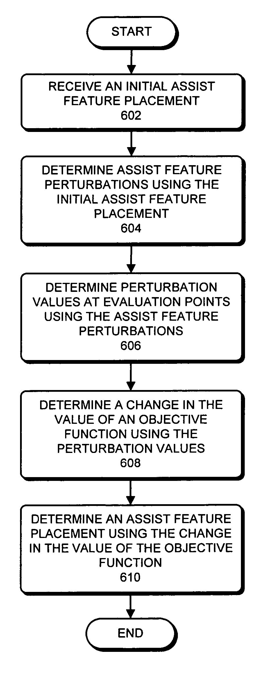
Assist feature placement using a process-sensitivity model
a technology of process sensitivity and feature placement, applied in the field of semiconductor manufacturing, can solve the problems of inability to accurately place assist features, inability to clean up, and/or sub-optimal placement of assist features, and require more wafer data for calibration and more effort on the part of engineers
- Summary
- Abstract
- Description
- Claims
- Application Information
AI Technical Summary
Benefits of technology
Problems solved by technology
Method used
Image

Examples
Embodiment Construction
Integrated Circuit Design Flow
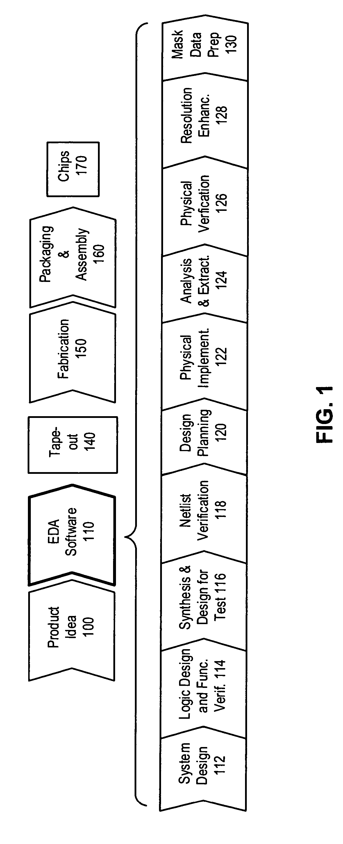
[0028]FIG. 1 illustrates various steps in the design and fabrication of an integrated circuit in accordance with an embodiment of the present invention.
[0029]The process starts with the product idea (step 100) which is realized using an EDA software design process (step 110). When the design is finalized, it can be taped-out (event 140). After tape out, the fabrication process (step 150) and packaging and assembly processes (step 160) are performed which ultimately result in finished chips (result 170).
[0030]The EDA software design process (step 110), in turn, comprises steps 112-130, which are described below. Note that the design flow description is for illustration purposes only. This description is not meant to limit the present invention. For example, an actual integrated circuit design may require the designer to perform the design steps in a different sequence than the sequence described below. The following discussion provides further details of...
PUM
 Abstract
Description
Claims
Application Information