MEMS microphone with a stacked PCB package and method of producing the same

a technology of pcb packages and microphones, applied in the field of packaging processes for a mems microphone and a stacked pcb package, can solve the problems of complex packaging requirements of a mems microphone or acoustic sensor, packaging is the biggest challenge in commercializing most mems devices, and the packaging of a mems device is totally different from packaging an integrated circuit, etc. cost

Active Publication Date: 2008-10-14
SHANDONG GETTOP ACOUSTIC
View PDF5 Cites 125 Cited by
  • Summary
  • Abstract
  • Description
  • Claims
  • Application Information

AI Technical Summary

Benefits of technology

[0010]A principal object of the present invention is to provide a cost-effective and very manufacturable method of producing a MEMS package incorporating a MEMS acoustic sensing device and one or more other electronic circuits.

Problems solved by technology

However, packaging of a MEMS device is totally different from packaging an integrated circuit.
Packaging is the biggest challenge for commercializing most MEMS devices.
The packaging requirements of a MEMS microphone or acoustic sensor are complex because the devices need to have an open path to receive sound pressure and yet the devices need to be protected from external environmental hazards like particles, dust, corrosive gases and humidity.
An insufficient back chamber will damp the diaphragm movement and increase the acoustic noise.
However, there is an insufficient back chamber behind the MEMS microphone / acoustic sensor. FIG. 1B illustrates another low cost package concept with a 2-layer PCB and a metal lid 104.
However, the opening 105 under the MEMS microphone / acoustic sensor 102 directly exposes the diaphragm to external environments, making it susceptible to external hazards.
However, this provides an insufficient back chamber, similar to the packaging concept illustrated in FIG. 1A.
However, the MEMS die may be exposed to external environmental hazards using this method.
Co-pending U.S. patent application (AL05-005) Ser. No. 11 / 333579, filed on Jan. 17, 2006, discloses the use of a metal meshed hole for environmental protection, but the flexible substrate and processing costs are still high.

Method used


Image

  • MEMS microphone with a stacked PCB package and method of producing the same
  • MEMS microphone with a stacked PCB package and method of producing the same
  • MEMS microphone with a stacked PCB package and method of producing the same

Examples


Embodiment Construction

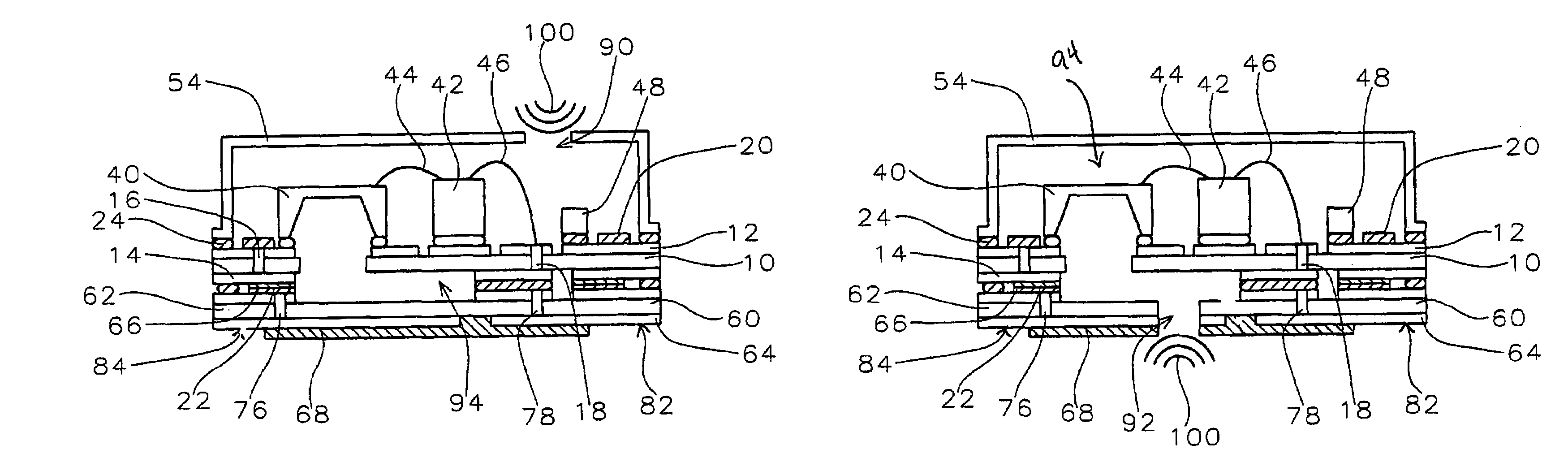
[0022]The present invention proposes a method for packaging a MEMS microphone or acoustic sensor device as well as one or more electronic components (typically, an application specific IC (ASIC) and one or more passive components) on a stacked PCB package. The present invention provides MEMS packages and a method of fabricating the MEMS packages that provide sufficient back chamber for the MEMS microphone and protection of the MEMS device from external environmental hazards while avoiding expensive substrate and packaging materials.

[0023]A first preferred embodiment of the invention is illustrated in FIG. 7. A second preferred embodiment of the invention is illustrated in FIG. 8. A preferred method to fabricate either the first or the second embodiment of the invention is illustrated in FIGS. 2-6.

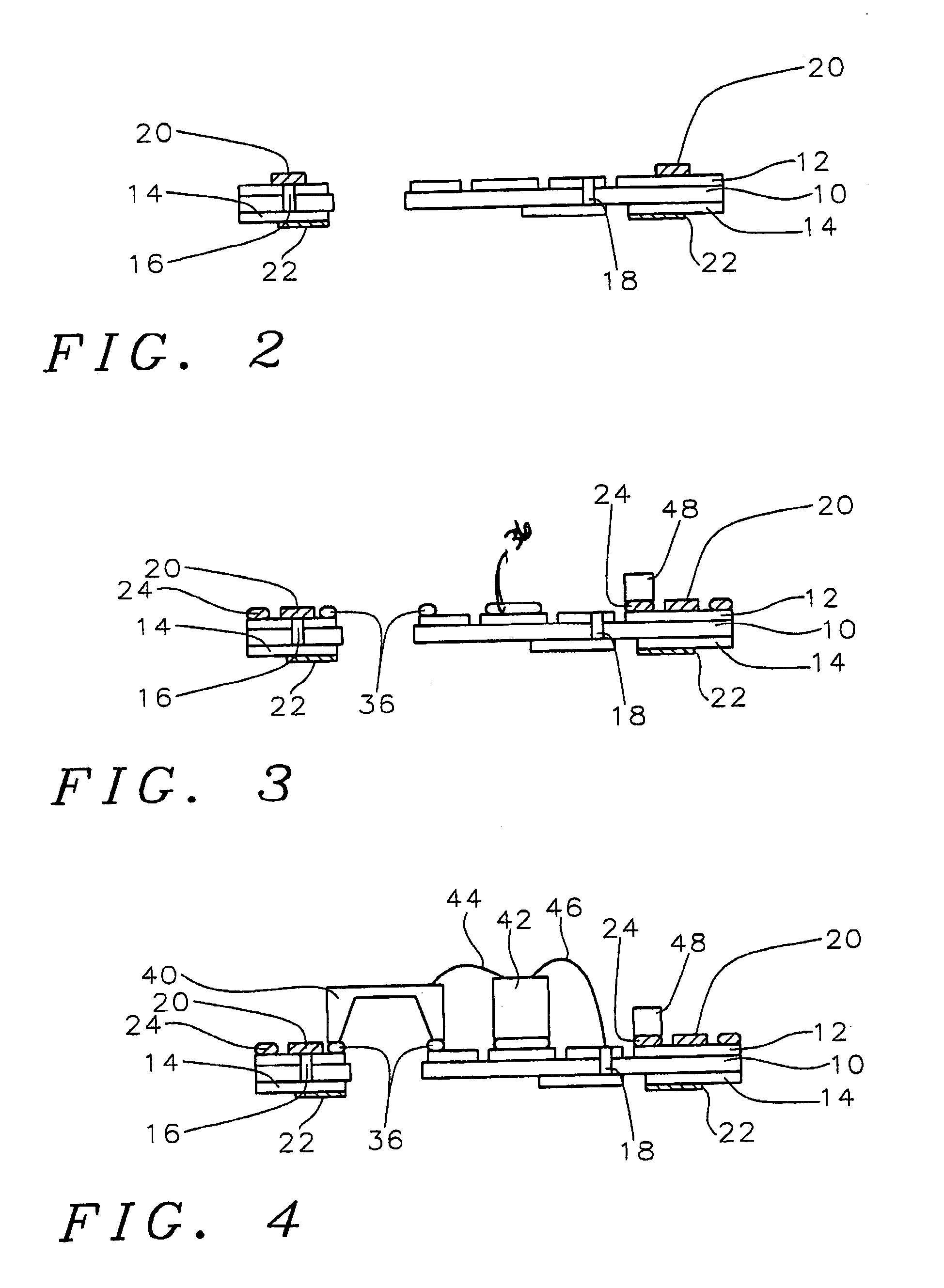
[0024]The preferred embodiment of the invention will now be described with reference to FIGS. 2 through 6. Referring now more particularly to FIG. 2, there is illustrated a two-layer printe...


PUM


Abstract

A MEMS microphone with a stacked PCB package is described. The MEMS package has at least one MEMS acoustic sensor device located on a PCB stack. A metal cap structure surrounds the at least one MEMS acoustic sensor device wherein an edge surface of the metal cap structure is attached and electrically connected to the PCB stack. In a first embodiment, a back chamber is formed underlying the at least one MEMS acoustic sensor device and within the PCB stack wherein an opening underlying the at least one MEMS acoustic sensor device accesses the back chamber. An opening in the metal cap structure not aligned with the at least one MEMS acoustic sensor device allows external fluid, acoustic energy or pressure to enter the at least one MEMS acoustic sensor device. In a second embodiment, a back chamber is formed in the space under the metal cap and over the first PCB. A hollow chamber is formed between the first PCB and the second PCB wherein an opening under the at least one MEMS acoustic sensor device accesses the hollow chamber. An opening in a bottom surface of the PCB stack not aligned with the at least one MEMS acoustic sensor device also accesses the hollow chamber and allows external fluid, acoustic energy or pressure to enter the at least one MEMS acoustic sensor device.

Description

BACKGROUND OF THE INVENTION[0001](1) Field of the Invention[0002]The invention relates to processes for packaging a MEMS microphone, and MEMS packages produced using the method, and more particularly, to a method of packaging a MEMS microphone having good environmental protection and a sufficient back chamber.[0003](2) Description of the Related Art[0004]Micro-electro-mechanical systems (MEMS) devices are known which convert physical phenomena, such as pressure, acceleration, sound, or light, into electrical signals. Each type of MEMS device interacts with the world in a different way, and demands custom or at least semi-custom packaging solutions. So-called system-in-package techniques attempt to form an entire microsystem—which could include a microprocessor, communications components, actuators and sensors—within a single package. However, packaging of a MEMS device is totally different from packaging an integrated circuit. MEMS devices are categorically different from ICs despit...

Claims


Application Information

Patent Timeline
Patent Type & Authority Patents(United States)
IPC IPC(8): H01L23/02
CPCB81C1/0023H01L24/83B81B2201/0257H01L2224/32225H01L2224/48091H01L2224/48137H01L2224/48227H01L2224/49109H01L2224/73265H01L2224/83192H01L2924/01078H01L2924/01079H01L2924/16152H01L2924/19041H01L2924/19105H01L2924/00014H01L2924/01087H01L2924/00H01L2224/45144H01L2924/01029H01L2924/14
Inventor ZHE, WANG
Owner SHANDONG GETTOP ACOUSTIC
Why Eureka
Try Eureka