Liquid crystal display panel and liquid crystal display device

a liquid crystal display panel and display panel technology, applied in non-linear optics, instruments, optics, etc., can solve the problem that the conventional lcd device fails to meet the wide view angle specification requirement, and achieve the effect of increasing the maximum contrast and effectively advanced viewing angle rang

Active Publication Date: 2008-10-21
WUHAN CHINA STAR OPTOELECTRONICS TECH CO LTD
View PDF4 Cites 0 Cited by
  • Summary
  • Abstract
  • Description
  • Claims
  • Application Information

AI Technical Summary

Benefits of technology

[0007]Accordingly, an object of the present invention is to provide a LCD panel with an increased viewing angle range.
[0008]Another object of the present invention is to provide a LCD panel with an improved maximum contrast ratio.
[0018]Based on the above, in the active component array substrate of the LCD panel and the LCD device of the present invention, since the included angle between the first orientation direction of the first alignment layer and the first line is between 46 and 74 degree, therefore, the viewing angle range can be effectively advanced to meet the wide view angle specification requirement. In addition, compared with the prior art, the LCD panel and the LCD device of the present invention possess a larger maximum contrast.

Problems solved by technology

Thus, the conventional LCD device fails to meet the wide view angle specification requirement.

Method used


Image

  • Liquid crystal display panel and liquid crystal display device
  • Liquid crystal display panel and liquid crystal display device
  • Liquid crystal display panel and liquid crystal display device

Examples


Embodiment Construction

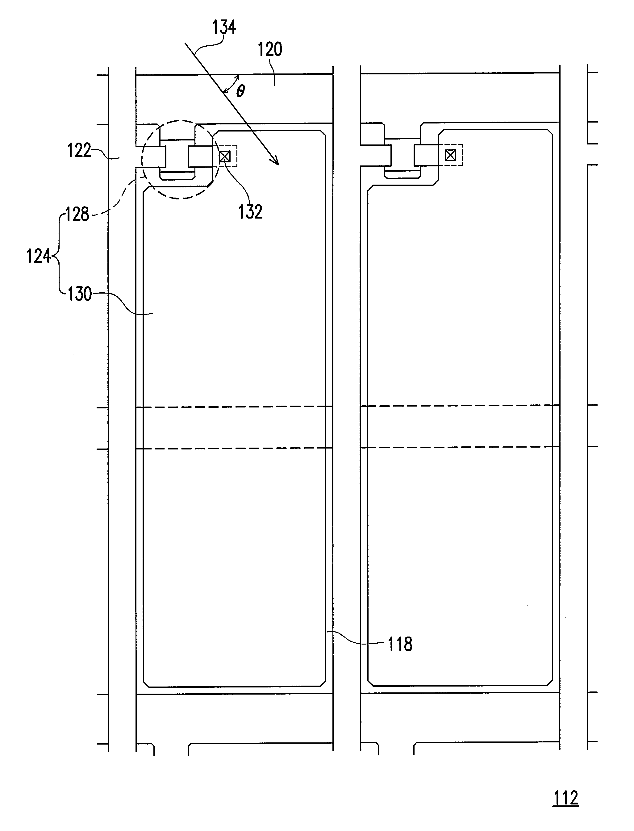
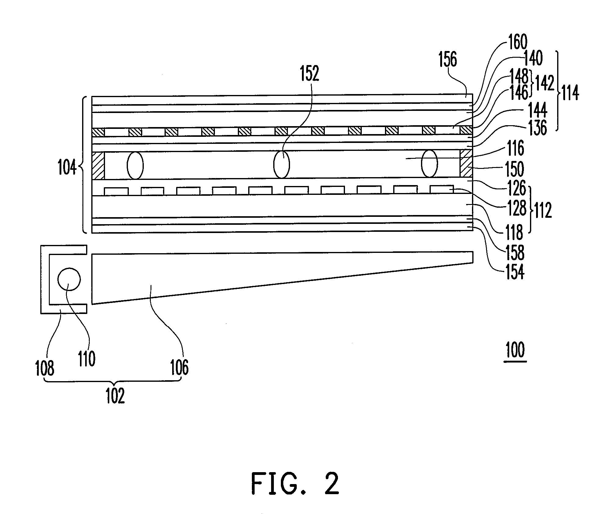
[0026]FIG. 2 is a schematic cross-sectional view of a LCD device according to an embodiment of the present invention, FIG. 3 is a schematic top view of an active component array substrate according to an embodiment of the present invention and FIG. 4 is a diagram of a LCD panel according to an embodiment of the present invention.

[0027]Referring to FIG. 2, a LCD device 100 of the present embodiment includes a backlight module 102 and a LCD panel 104. Wherein, the backlight module 102 includes, for example, a light guide plate (LGP) 106, a reflective lampshade 108 and a light source 110. In more detail, the LGP 106 can be a wedge-shaped light guide plate. The reflective lampshade 108 is disposed at the side of the light incident end of the LGP 106 (not shown), while the light source 110 is disposed in the reflective lampshade 108. The above-described light source 110 can be a cold cathode fluorescence lamp (CCFL) or a light-emitting diode array (LED array), both of which are suitable ...


PUM

PropertyMeasurementUnit
included angleaaaaaaaaaa

Abstract

A liquid crystal display panel (LCD panel) includes an active component array substrate, an opposite substrate and an optically compensated birefringence type liquid crystal layer (OCB-type liquid crystal layer). The active component array substrate includes a first substrate, a plurality of first lines, a plurality of second lines, a plurality of pixel structures and a first alignment layer. The first alignment layer possesses a first orientation direction, and the included angle between the first orientation direction and the first lines is between 46 and 74 degree. The opposite substrate has a second alignment layer facing the active component array substrate, and the second alignment layer possesses a second orientation direction parallel to the first orientation direction. The OCB-type liquid crystal layer is disposed between the active component array substrate and the opposite substrate.

Description

BACKGROUND OF THE INVENTION[0001]1. Field of Invention[0002]The present invention relates to a liquid crystal display panel (LCD panel) and a liquid display crystal device (LCD device), and particularly to a LCD panel and a LCD device of optically compensated birefringence type (OCB-type).[0003]2. Description of the Related Art[0004]LCD devices can be categorized into different types according to liquid crystal type, driving method and light source disposition. Wherein, an OCB-type LCD device has advantage such as fast response speed, and is suitable for providing a computer with excellent and smooth frame performance, where fast-varied sequential frames are essential to play an animation or a movie. Therefore, an OCB-type LCD device usually serves as a high-end LCD device. For an OCB-type LCD device to have a fast response performance, however, the optically compensated birefringence liquid crystal molecules (OCB liquid crystal molecules) thereof must be transited from splay state ...

Claims


Application Information

Patent Timeline
Patent Type & Authority Patents(United States)
IPC IPC(8): G02F1/1337
CPCG02F1/1337G02F1/1395
Inventor SYU, CHAO-DONGYANG, SHIH-TSUNGPAN, CHIEN-LINHU, KUAN-CHIUNTIEN, HAO-TING
Owner WUHAN CHINA STAR OPTOELECTRONICS TECH CO LTD
Why Eureka
Try Eureka