Touch control panel and manufacturing method thereof

a technology of touch control panel and manufacturing method, which is applied in the field of display technology, can solve the problems of limiting the brightness/chromaticity of the display, and the viewing angle range of the oled display will inevitably be further affected, so as to achieve the effect of increasing the viewing angle range of the oled display

Active Publication Date: 2021-05-27
WUHAN CHINA STAR OPTOELECTRONICS SEMICON DISPLAY TECH CO LTD
View PDF0 Cites 1 Cited by
  • Summary
  • Abstract
  • Description
  • Claims
  • Application Information

AI Technical Summary

Benefits of technology

[0007]An embodiment of the present invention provides a touch control panel and a manufacturing method thereof. By arranging an insulating layer between a first metal layer and a second metal layer whose elastic modulus different from an adjacent inorganic layer or organic layer, their contact surface is made lumpy. When light emitted by an EL layer reaches the lumpy contact surface, refraction of different angles occurs, which thereby increases a range of viewing angles of OLEDs.
[0018]An embodiment of the present invention, by arranging an insulating layer with elastic modulus different from an adjacent inorganic layer or organic layer between a first metal layer and a second metal layer, makes their contact surfaces uneven. When light emitted by an EL layer reaches the uneven contact surfaces, refraction of different angles occurs, thereby increasing a viewing angle range of OLEDs.

Problems solved by technology

Light emitted by the EL layer passing the anode layer at a bottom of the EL layer is usually linearly emitted upward, and therefore its viewing angles of brightness / chromaticity are usually limited.
However, if a metal mesh touch sensing unit is integrated on the OLED display, a viewing angle range of the OLED display will inevitably be further affected, particularly by a light-shading property of metal meshes.

Method used


Image

  • Touch control panel and manufacturing method thereof
  • Touch control panel and manufacturing method thereof
  • Touch control panel and manufacturing method thereof

Examples


Embodiment Construction

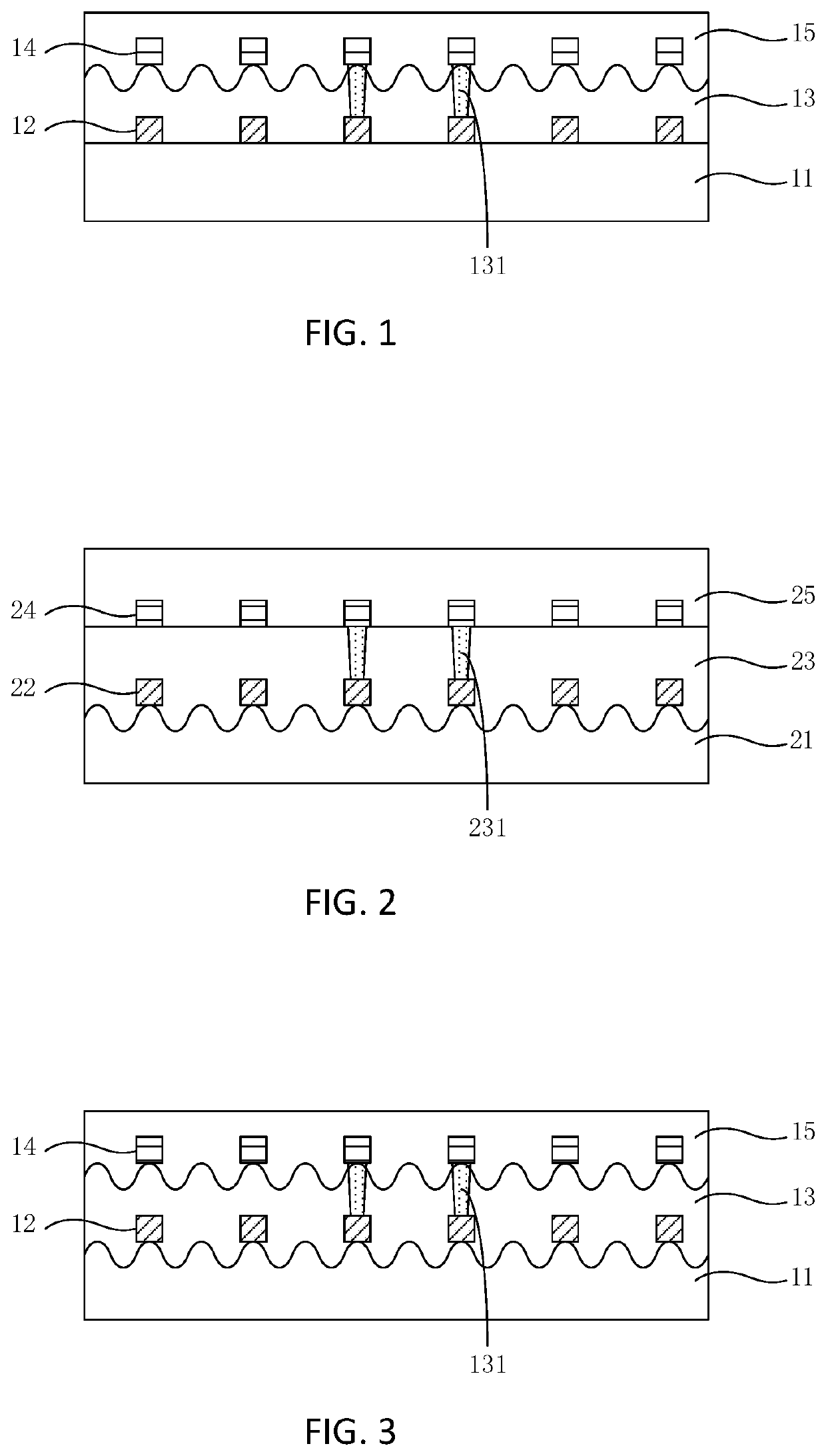
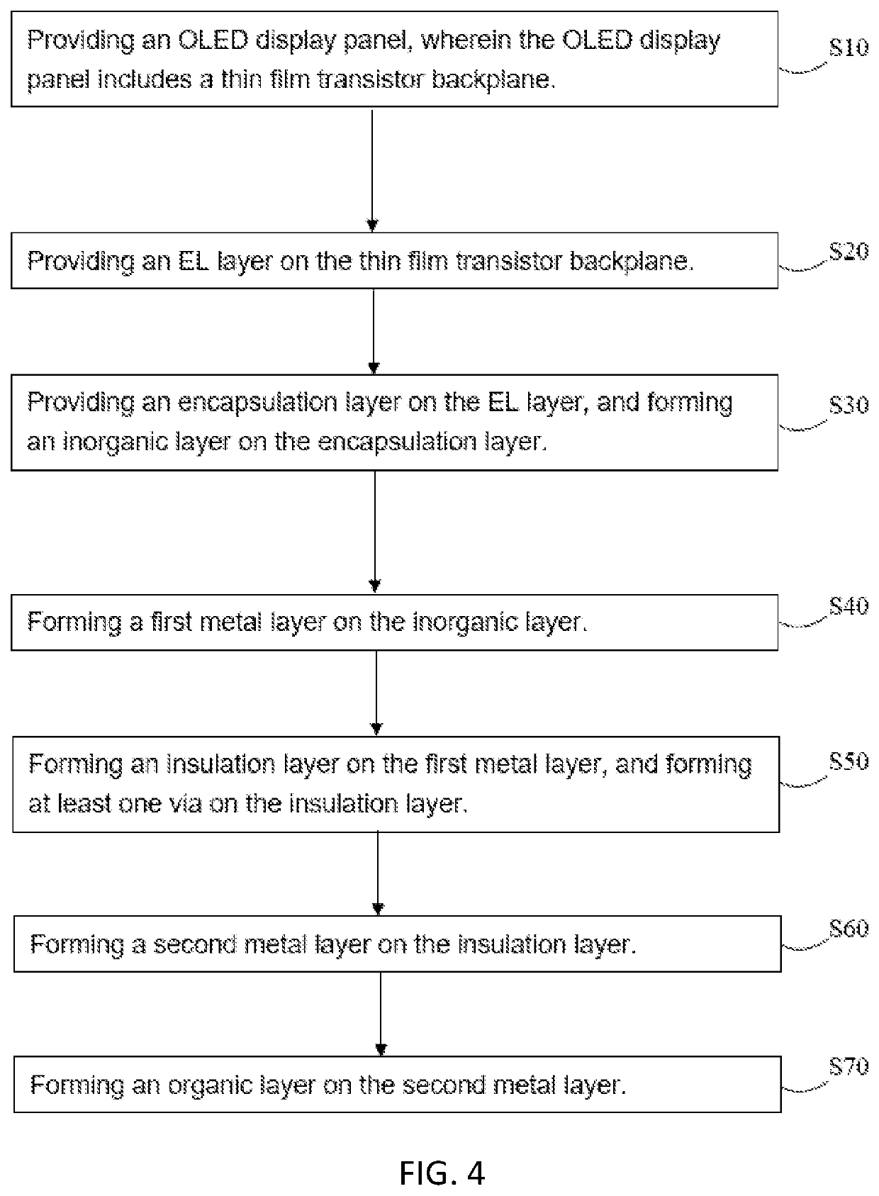
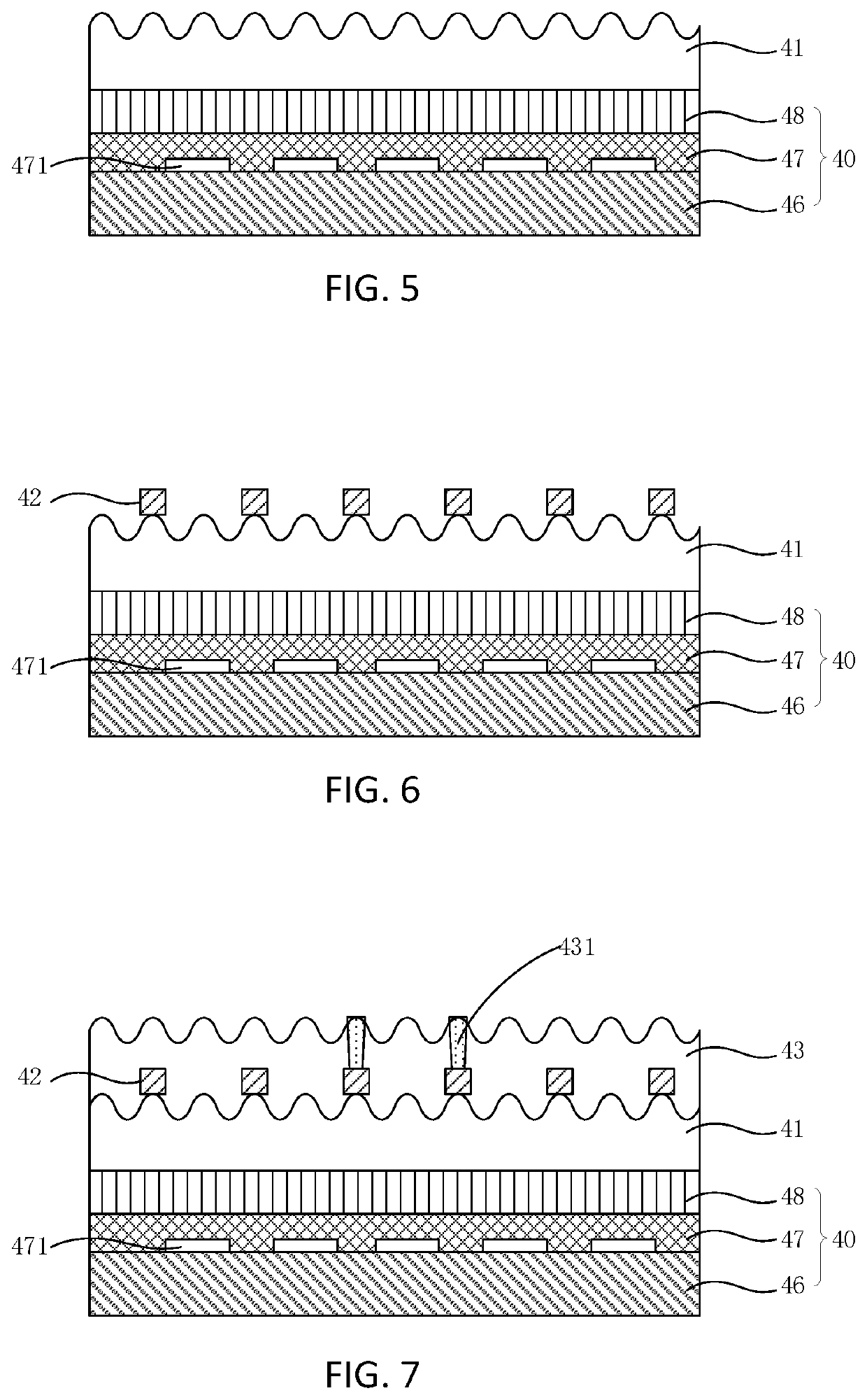
[0025]The embodiments of the present invention are described in detail hereinafter. Examples of the described embodiments are given in the accompanying drawings. It should be noted that the following embodiments are intended to illustrate and interpret the present invention, and shall not be construed as causing limitations to the present invention. Similarly, the following embodiments are part of the embodiments of the present invention and are not the whole embodiments, and all other embodiments obtained by those skilled in the art without making any inventive efforts are within the scope protected by the present invention.

[0026]Terms such as “first”, “second”, “third”, etc. (if they exist) in the specification, claim and above-mentioned drawings of the present invention are used herein for purposes of description and are not intended to indicate or imply relative order or significance. It should be understood that elements described by such terms can be switched under proper cond...


PUM

PropertyMeasurementUnit
elastic modulusaaaaaaaaaa
electroluminescentaaaaaaaaaa
brightnessaaaaaaaaaa

Abstract

The present invention provides a touch control panel and a manufacturing method thereof. The present invention, by arranging an insulating layer with elastic modulus different from an adjacent inorganic layer or organic layer between a first metal layer and a second metal layer, makes their contact surfaces uneven. When light emitted by an electroluminescent (EL) layer reaches the uneven contact surfaces, refraction of different angles occurs, thereby increasing a viewing angle range of organic light-emitting diodes (OLEDs).

Description

FIELD OF INVENTION[0001]The present invention relates to the field of display technology, and especially to a touch control panel and a manufacturing method thereof.BACKGROUND OF INVENTION[0002]Flexible organic light-emitting diode (OLED) displays have advantages such as self-luminescence, wide color gamut, high brightness, quick response times, low power consumption, bendable structures, etc., and have become increasingly popular in the market, gradually replacing liquid crystal displays (LCDs) to become a mainstream of display technology.[0003]Flexible OLEDs are divided into two categories of top emission and bottom emission according to their light-emitting position. Currently, top emission is the mainstream of OLED mass production technology. It has a bottom-up structure that sequentially includes a thin-film transistor (TFT) array substrate, an anode layer, a pixel defining layer (PDL), an electroluminescent (EL) layer, a cathode layer, a thin-film encapsulation (TFE) layer, an...

Claims


Application Information

Patent Timeline
Patent Type & Authority Applications(United States)
IPC IPC(8): H01L27/32H01L51/56H01L51/52H01L51/50
CPCH01L27/323H01L51/56H01L2251/301H01L51/5012H01L27/3244H01L51/5237G06F3/0412G06F2203/04103H10K59/40H10K50/858H10K59/1201H10K50/11H10K50/84H10K59/12H10K71/00H10K2102/00
Inventor YE, JIAN
Owner WUHAN CHINA STAR OPTOELECTRONICS SEMICON DISPLAY TECH CO LTD
Why Eureka
Try Eureka