Radiation-emitting semiconductor chip, method for production thereof and radiation-emitting component

Inactive Publication Date: 2008-11-04
OSRAM OPTO SEMICON GMBH & CO OHG
View PDF23 Cites 38 Cited by
  • Summary
  • Abstract
  • Description
  • Claims
  • Application Information

AI Technical Summary

Benefits of technology

[0029]One object of the invention is to provide a radiation-emitting semiconductor chip of the type mentioned in the introduction with improved coupling-out of light, which is suitable for the mass production of light-emitting diode components, and in which

Problems solved by technology

In this case, a major difficulty is posed by the great difference between the refractive indices of customary semiconductor materials of optical semiconductor elements (n>2.5) and the conventionally available potting materials (for example epoxy resin; nEpoxy≅1.5).
This is the reason why, on account of total reflection at the chip surfaces, a considerable part of the light generated in the active zone is not coupled out from the semiconductor body and is lost in the interior thereof.
Given a predetermined electric current which flows through the semiconductor component for the purpose of generating the light, the brightness of the component is thus limited.
In the case of GaN-based light-emitting diode chips in which the epitaxial layer sequence is arranged on a substrate (for example a silicon carbide substrate) which has a higher refractive index than the epitaxial layer sequence, the particular problem arises, moreover, that, given a conventional parallelepipedal chip geometry, the proportion of radiation which is coupled out through the substrate flanks is coupled out at a very acute angle with respect to the substrate flank in the direction of the rear side of the chip.
This entails the disadvantages that, firstly, on account of the acute angle of incidence, a large part of the radiation is absorbed in the chip mounting area and, secondly, there is a considerable risk of a certain part of the radiation impinging on the conductive adhesive usually used for fixing the chip and being absorbed by said conductive adhesive.
This known chip geometry, which is primarily directed at improving the coupling-out of light via the front side, raises the following problems, in particular:(i) During the production of the oblique side areas, a considerable proportion of the area of the active epitaxial layer sequence present on the wafer is lost because these are produced by means of the production of a V-shaped trench from the side of the active zone.(ii) The thickness of the secondary window layer is greatly limited in order that a sufficiently large chip mounting area is preserved, in the case of whichthe chip is not tilted in the course of its mounting in a light-emitting diode housing,a current expansion to as far as

Method used


Image

  • Radiation-emitting semiconductor chip, method for production thereof and radiation-emitting component
  • Radiation-emitting semiconductor chip, method for production thereof and radiation-emitting component
  • Radiation-emitting semiconductor chip, method for production thereof and radiation-emitting component

Examples


Example

DETAILED DESCRIPTION OF THE DRAWINGS

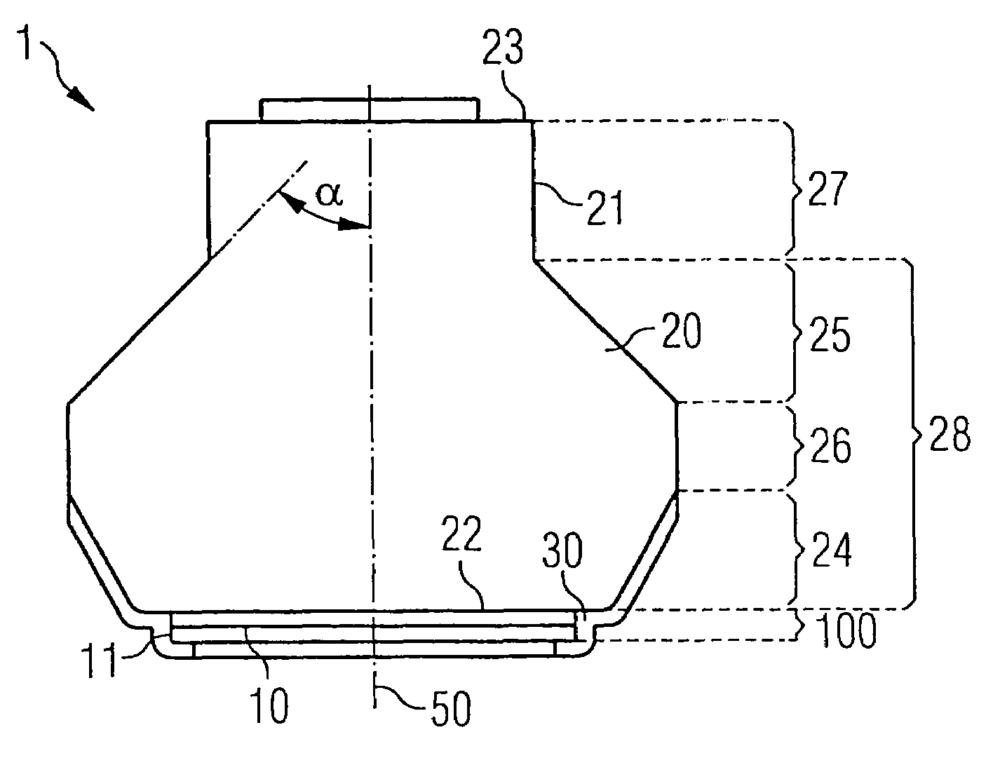
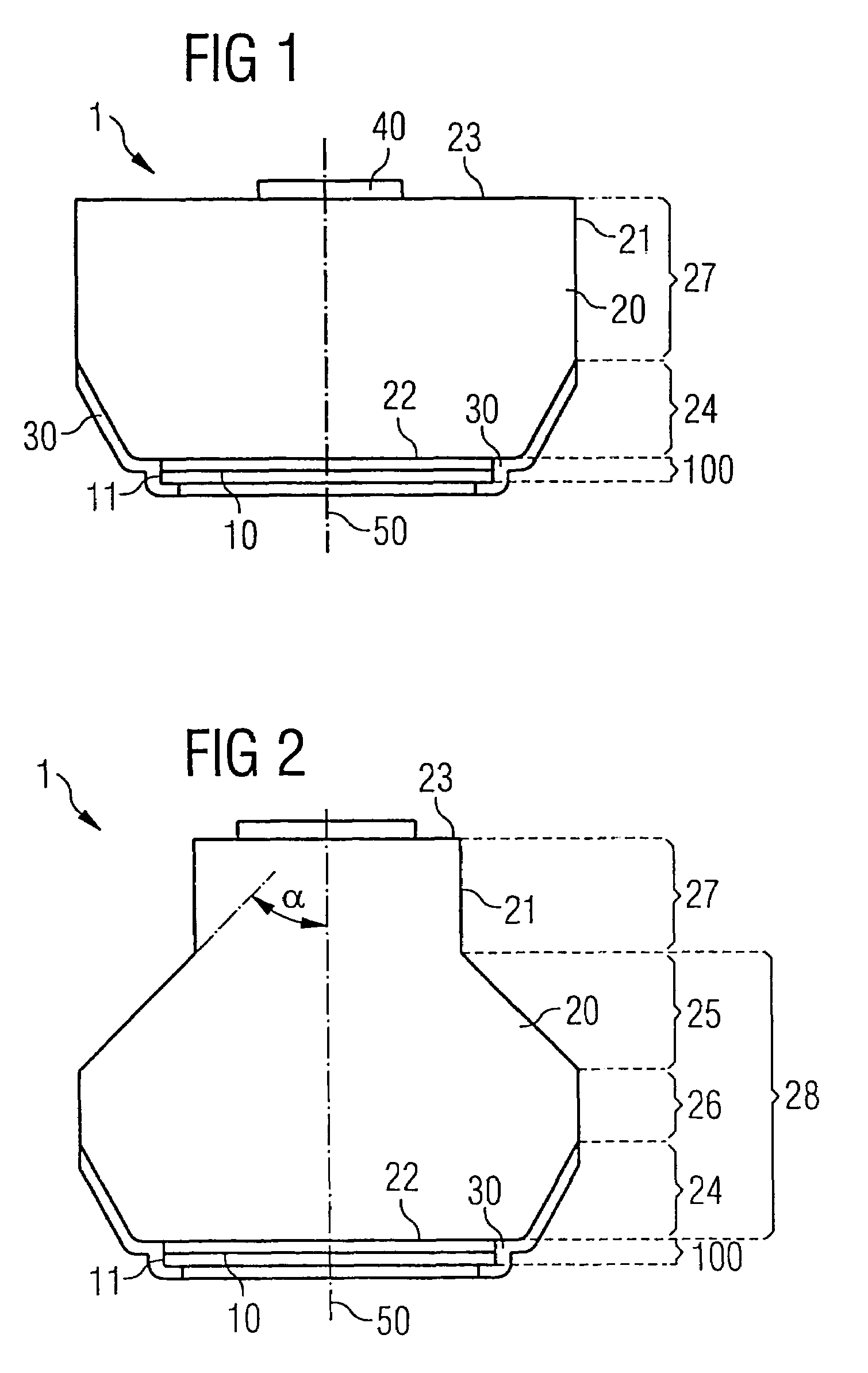
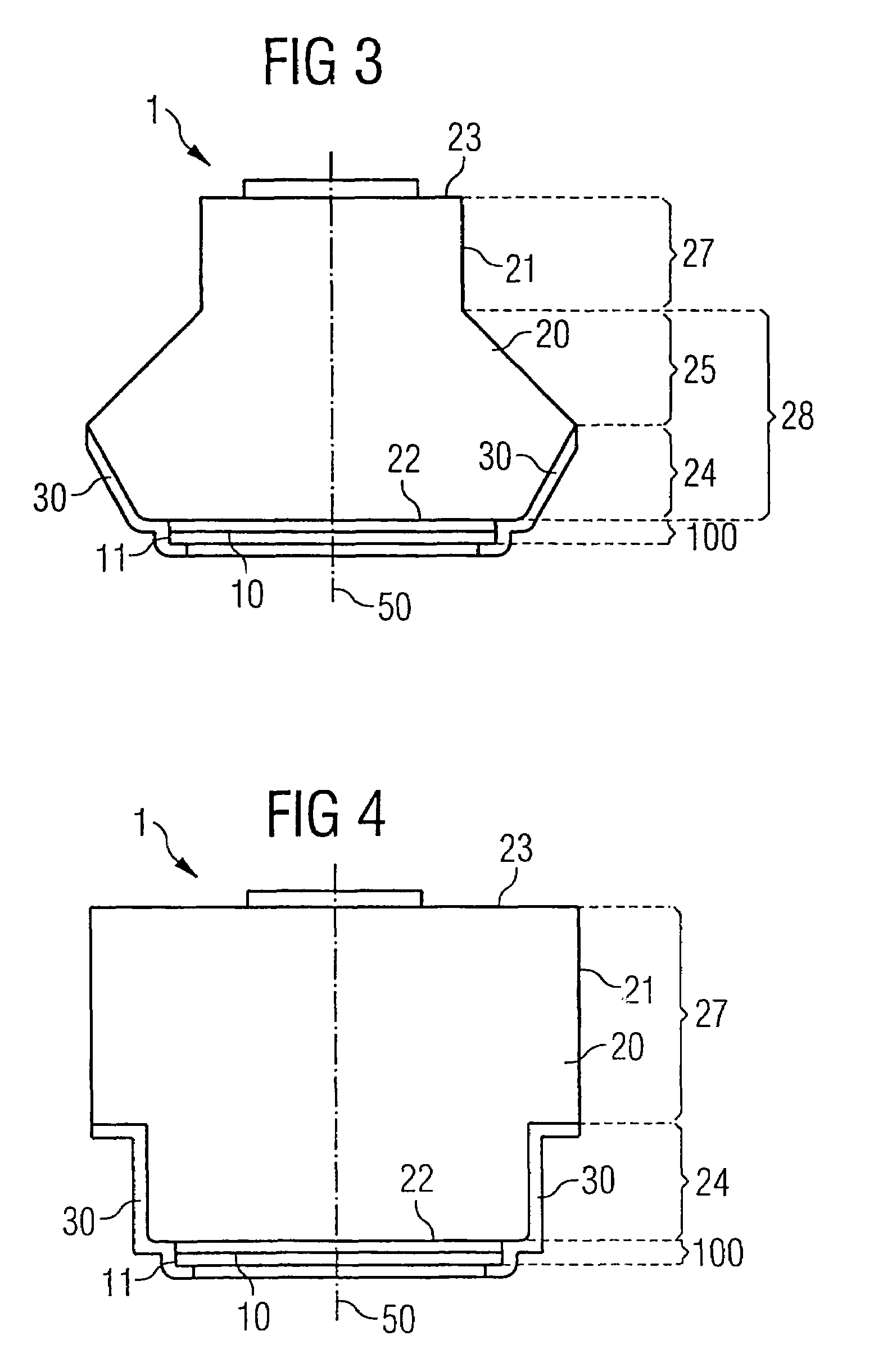
[0078]In the Figures, respectively identical or identically acting constituent parts of the exemplary embodiments are in each case provided with the same reference symbols.

[0079]FIG. 1 shows purely diagrammatically a cross section through a radiation-emitting semiconductor chip 1 according to the invention. An active layer 10 that generates the light, for example a single quantum well (SQW) or multiple quantum well (MQW) structure based on InGaN, lies within a multilayer structure 100, which, by way of example, comprises overall a plurality of nitride-based semiconductor layers. The precise construction of such a multilayer structure is dependent on the material system and the desired properties of the component. Details in this respect are disclosed in the prior art and therefore are not explained in any further detail in the present context.

[0080]The multilayer structure 100 is produced for example by metal organic vapor phase epitaxy methods on...


PUM


Abstract

A radiation-emitting semiconductor chip, having a multilayer structure (100) containing a radiation-emitting active layer (10), and having a window layer (20), which is transmissive to a radiation emitted by the active layer (10) and is arranged downstream of the multilayer structure (100) in the direction of a main radiating direction of the semiconductor component. The window layer (20) has at least one peripheral side area (21), which, in the course from a first main area (22) facing the multilayer structure (100) in the direction toward a second main area (23) remote from the multilayer structure (100), firstly has a first side area region (24) which is beveled, curved or stepped in such a way that the window layer widens with respect to the size of the first main area (22). A peripheral side area (11) of the multilayer structure (100) and at least a part of the beveled, curved or stepped first side area region (24) are coated with a continuous electrically insulating layer (30). A radiation-emitting component is disclosed having a chip of this type, and also disclosed is a method for simultaneously producing a multiplicity of such chips.

Description

RELATED APPLICATIONS[0001]This is a U.S. national stage of International application No. PCT / DE02 / 03668 filed on 27 Sep. 2002.[0002]This patent application claims priority of German patent application No. 10148227.2 filed 28 Sep. 2001, the disclosure of which is hereby incorporated by reference.FIELD OF THE INVENTION[0003]The invention relates to a radiation-emitting semiconductor chip having a multilayer structure containing a radiation-emitting active layer, and having a window layer, which is transmissive to a radiation emitted by the active layer and is arranged downstream of the multilayer structure in the direction of a main radiating direction of the semiconductor component. It furthermore relates to a method for producing such a semiconductor chip and to a radiation-emitting component having such a semiconductor chip.[0004]The invention relates, in particular, to a radiation-emitting semiconductor chip having a nitride-based radiation-emitting active multilayer structure app...

Claims


Application Information

Patent Timeline
IPC IPC(8): H01L33/00H01L33/20
CPCH01L33/20H01L24/32H01L2224/48247H01L2924/10155H01L2224/73265H01L2224/48091H01L2224/32245H01L2924/00014H01L2924/00H01L2924/12042H01L2924/12041
Inventor FEHRER, MICHAELHARLE, VOLKERKUHN, FRANKZEHNDER, ULRICH
Owner OSRAM OPTO SEMICON GMBH & CO OHG
Why Eureka
Try Eureka