Multi-level flash memory with temperature compensation

a flash memory and temperature compensation technology, applied in the field of flash memory devices, can solve the problems of affecting the reliability of data states, and sensitive threshold voltage profiles of flash memory,

Inactive Publication Date: 2005-03-22
SAMSUNG ELECTRONICS CO LTD
View PDF3 Cites 216 Cited by
  • Summary
  • Abstract
  • Description
  • Claims
  • Application Information

AI Technical Summary

Benefits of technology

According to one aspect of the present invention, a multi-level semiconductor memory device includes a plurality of wordlines and bitlines connected to memory cells that store multi-level data. A first circuit supplies a temperature-responsive voltage to a selected wordline to read a state of the memory cell. A second circuit supplies a predetermined

Problems solved by technology

However, the margin limits must also be considered because margins that are too large increase the threshold voltages of the highest distribution profile and also increase read voltages, regardless of program states.
A higher read voltage can cause a soft program, which degrades the reliability of data states.
Threshold voltage profiles of the flash memories are sensitive, however, to temperature variation during programming and reading.
However, referring to FIGS. 4B through 4D, when the programming and reading operations are carried out at temperatures different from each other, migration of the threshold profiles reduces the margins and causes reading failures.
This, in turn, causes a termination of the programming operation befo

Method used


Image

  • Multi-level flash memory with temperature compensation
  • Multi-level flash memory with temperature compensation
  • Multi-level flash memory with temperature compensation

Examples


Embodiment Construction

Various embodiments of the invention will now be explained with reference to FIGS. 5 through 11. It should be understood, however, that the following description of preferred embodiments is illustrative only, and should not be taken in a limiting sense. Although specific details are set forth in order to provide a more thorough understanding of the principles of the present invention, it will be apparent to those skilled in the art that those principles may be practiced in any of a number of different ways.

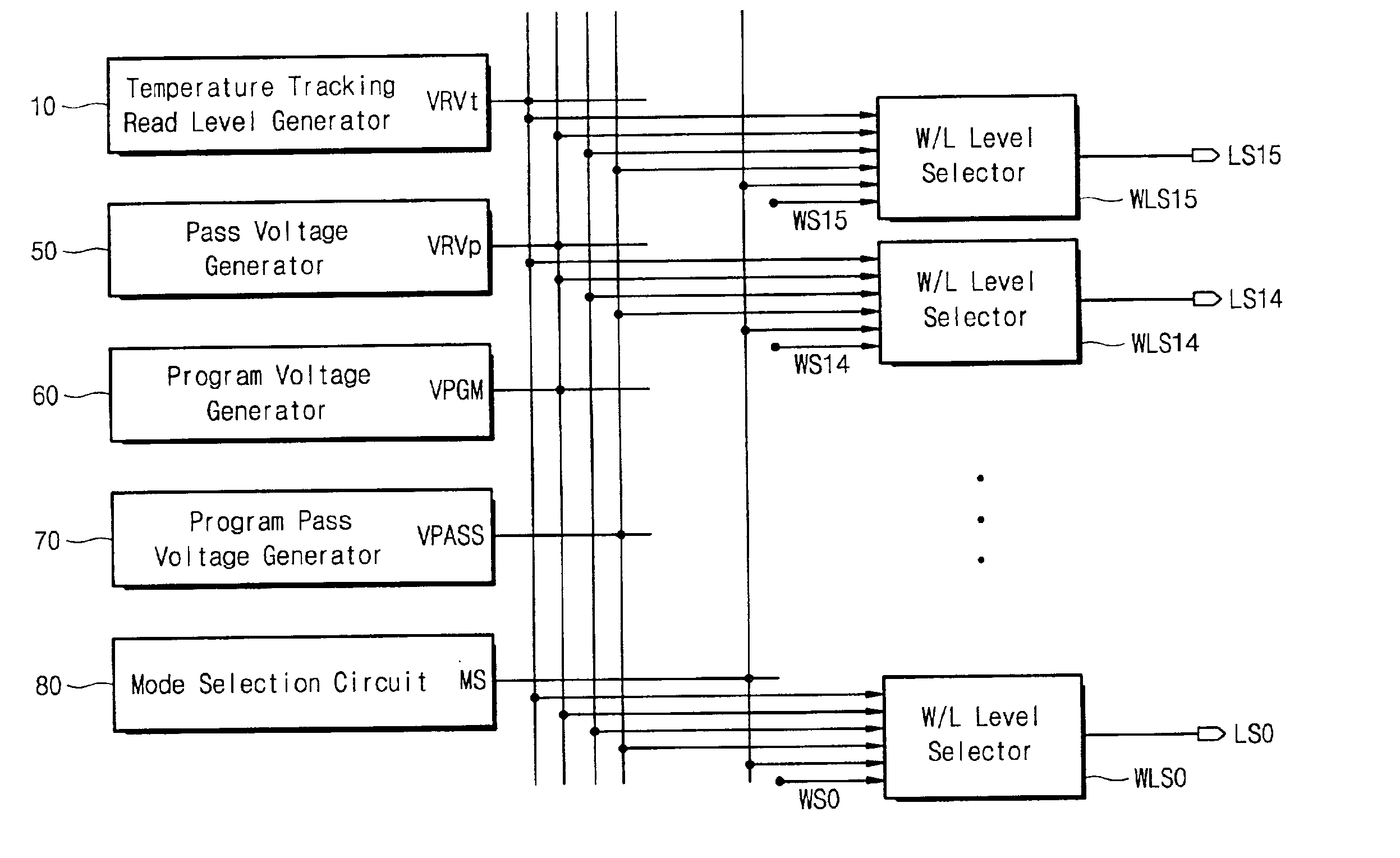
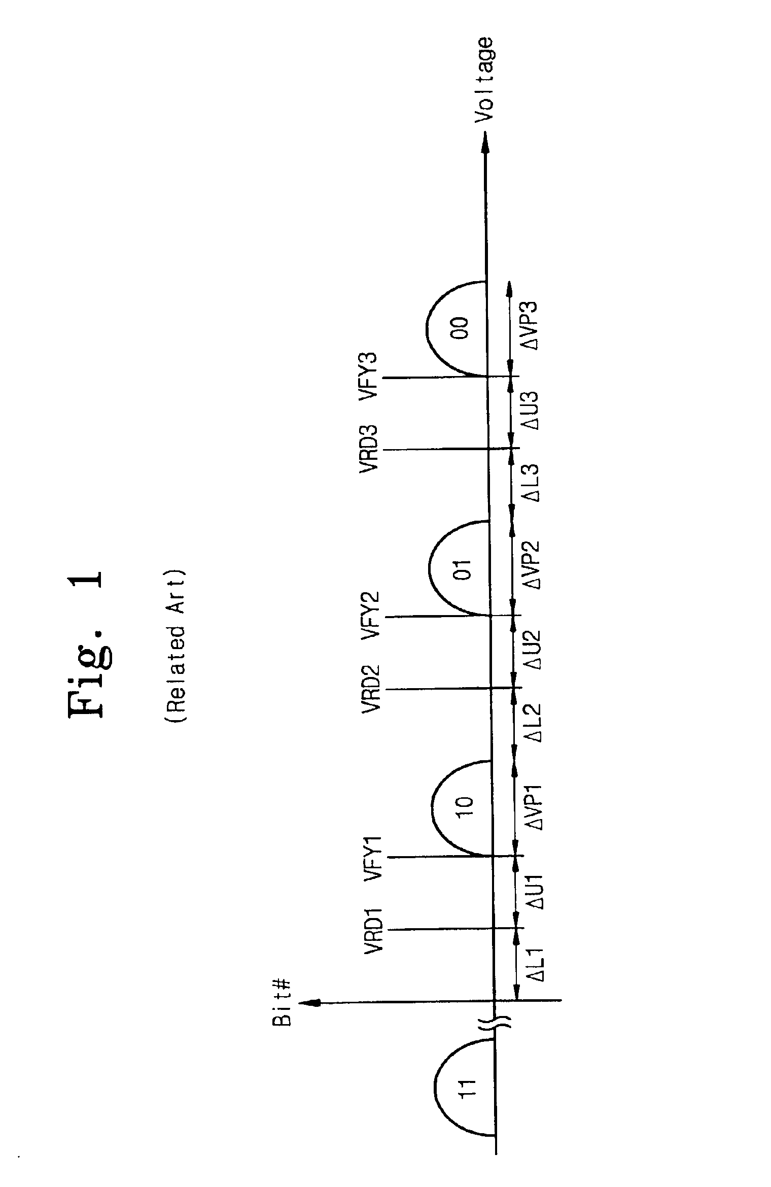
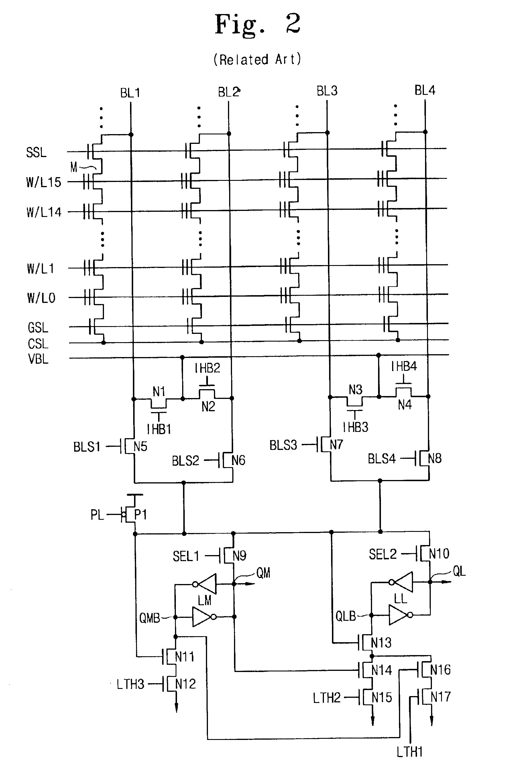
In general, a NAND-type multi-level flash memory includes a memory cell array having a plurality of memory cells. Each of the memory cells can be set in one of four, two-bit data states (i.e., “11”, “10”, “01”, or “00”). Peripheral circuits load data into and sense data from the memory cells. Each memory cell has floating and control gates that are isolated from each other by an insulation film, as well as source and drain regions that are formed in a semiconductor substrate. Eras...


PUM


Abstract

A multi-level semiconductor memory device preferably includes a plurality of wordlines connected to memory cells configured to store multi-level data. A first circuit supplies a temperature-responsive voltage to a selected wordline in order to read a state of a selected memory cell. A second circuit supplies a predetermined voltage to non-selected wordlines. The first circuit preferably includes a semiconductor element that varies its resistance in accordance with temperature. Reliable program-verifying and reading functions are preferably provided despite migration of threshold voltage distribution profiles due to temperature variations.

Description

This application claims priority from Korean Patent Application 2002-18448, the contents of which are incorporated herein by reference in their entirety.BACKGROUND OF THE INVENTION1. Field of the InventionThe present invention relates generally to flash memory devices and, more specifically, to multi-level flash memory devices.2. Description of Related ArtFlash memories (e.g., flash EEPROMs) are useful as subsidiary storage elements because they are capable of providing a large memory capacity with a higher degree of integration than traditional EEPROMs. NAND-type flash memories, in particular, typically have a higher integration density than other types of flash memories such as NOR- or AND-types. A memory cell of a flash memory is typically constructed by forming source and drain regions in a semiconductor substrate, forming a thin oxide film on the surface of the substrate between the source and drain regions, and then forming a floating gate, an interlayer oxide film, and a cont...

Claims


Application Information

Patent Timeline
IPC IPC(8): G11C11/56G11C8/00G11C8/08G11C16/06G11C16/02G11C16/04
CPCG11C7/04G11C8/08G11C16/3459G11C11/5642G11C16/06G11C11/5628
Inventor CHO, TAE-HEELEE, YEONG-TAEK
Owner SAMSUNG ELECTRONICS CO LTD
Why Eureka
Try Eureka