Wiring board embedded with spherical semiconductor element

a technology of spherical semiconductor elements and wiring boards, which is applied in the direction of semiconductor devices, semiconductor/solid-state device details, semiconductor devices, etc., can solve the problems of limited spherical semiconductor element use regions, limited spherical semiconductor element use areas, and many wiring constraints

Inactive Publication Date: 2007-03-29
PANASONIC CORP
View PDF6 Cites 211 Cited by
  • Summary
  • Abstract
  • Description
  • Claims
  • Application Information

AI Technical Summary

Benefits of technology

[0092] Further, by providing with the flexibility while making a predetermined region rigidized, a required flexibility can be provided to a specific region of the wiring board. As a result, the wiring board can be housed in a housing of for example a mobile phone while its form follows inner profile of the housing. That is, the wiring board can be contained in the housing without formation of a useless space in the housing, which is convenient for the miniaturizing and thinning of the electronic device.

Problems solved by technology

As far as the surface mounting is used, the number of the bumps which connect the spherical semiconductor element to a multilayer wiring board is limited, which leads to a number of constraints as to wiring.
On the other hand, when considering that a passive element is formed in a device, a passive element other than an inductor element is formed in or on a substrate, or a passive element is surface-mounted, which causes a considerable constraint upon the formation of a wiring, so that there are a number of problems when the spherical semiconductor element is used for a variety of applications.
As a result, a region where the spherical semiconductor element is used is limited.
This means that it is impossible to construct an design having a function while exploiting the thickness of the spherical semiconductor element.
That is, in the prior art, since the spherical semiconductor element is surface-amounted, such design is impossible.
In such embodiment, there is a constraint as to the design in for example that even the smallest pitch between the via hole conductors should be larger than a diameter of a land electrode such as 1302c or 1302d which is located at the end of the via hole conductor, so that miniaturizing of the substrate size, and thus making the higher density has limitations.
Further, since the wiring board is formed with using a thermosetting resin and a fabric such as a non-woven fabric, the wiring board is rigid as a whole and it is impossible to arbitrarily inflected it, which makes it difficult to contain the wiring board in a limited space of an electronic device which should be miniaturized and thin.

Method used


Image

  • Wiring board embedded with spherical semiconductor element
  • Wiring board embedded with spherical semiconductor element
  • Wiring board embedded with spherical semiconductor element

Examples


first embodiment

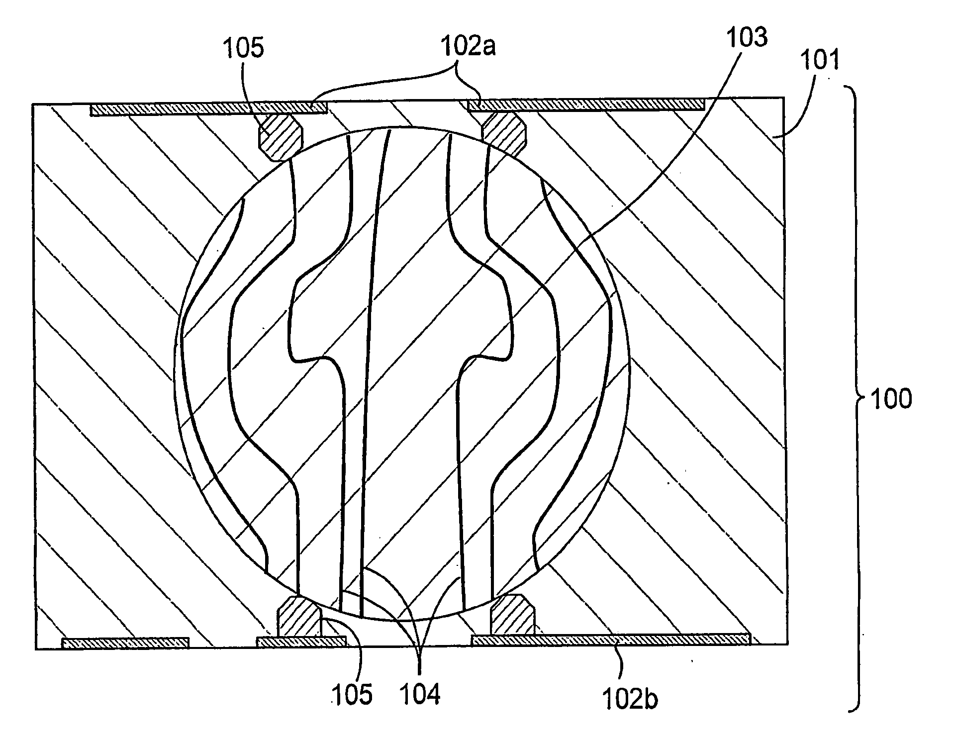
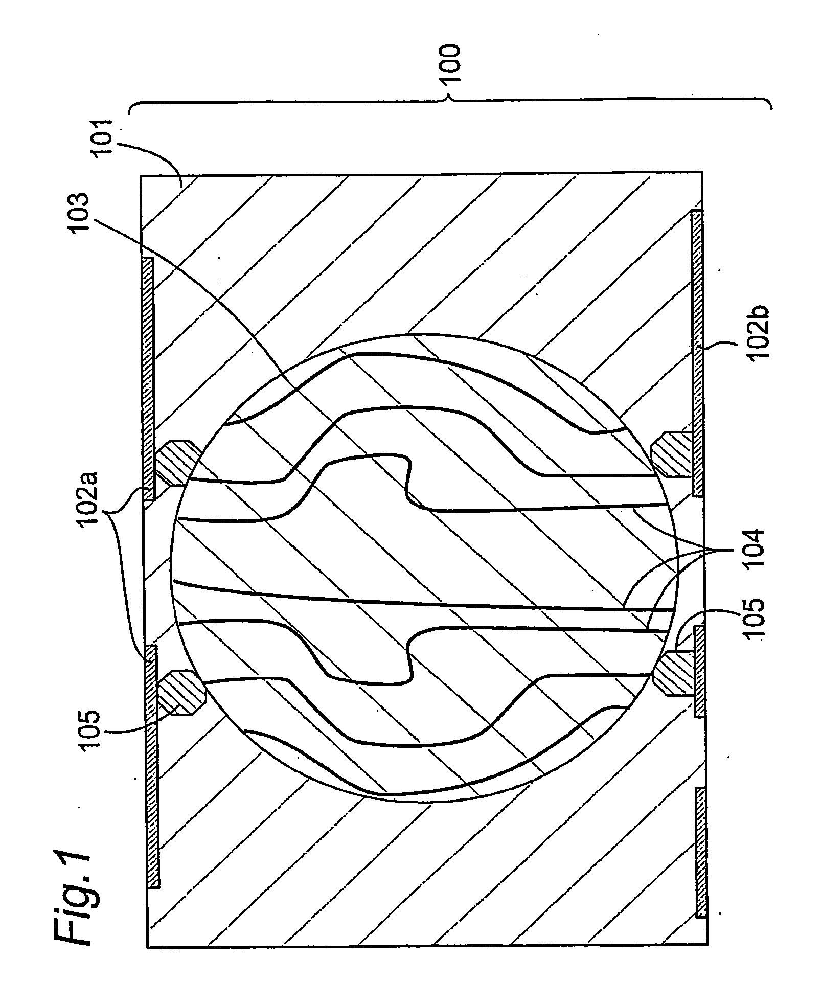
[0124] The first embodiment is an example of a wiring board according to the present invention which comprises a spherical semiconductor element, which is shown in a schematic cross sectional view in FIG. 1.

[0125] As shown in FIG. 1, the wiring board 100 comprises an electrically insulating substrate 101, a wiring pattern 102a which is formed on one main surface of the electrically insulating substrate 101, a wiring pattern 102b which is formed on the other main surface of the electrically insulating substrate 101, and a spherical semiconductor element 103 which is embedded in the inside of the electrically insulating substrate 101. The wiring patterns 102a and 102b are electrically connected through wirings 104 which are formed on the spherical semiconductor element as well as bumps 105 which are formed on terminal electrodes (not shown) of the wirings. In the shown embodiment, the wiring patterns and the wirings are electrically connected directly.

[0126] The electrically insulat...

second embodiment

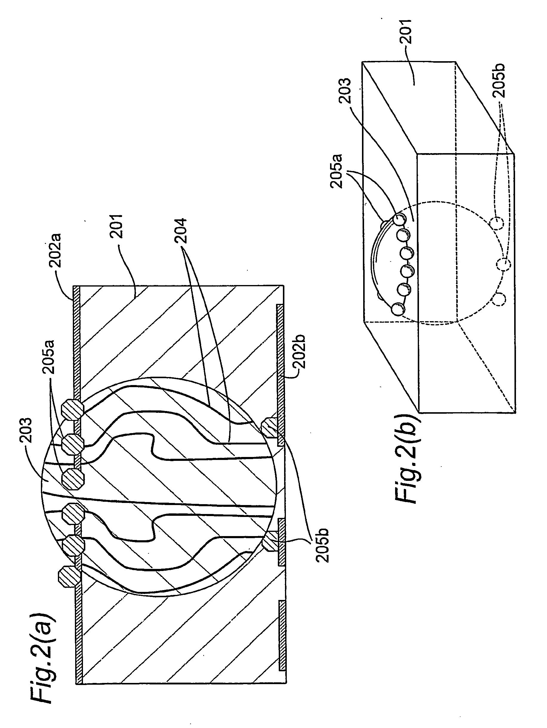
[0136] The second embodiment is one example of a wiring board according to the present invention which comprises a spherical semiconductor element and a passive element, which is shown in a schematic cross sectional view in FIG. 3. The wiring board 300 of the present embodiment corresponds to the wiring board as shown which further comprises the passive element 306, and such wiring board comprises an electrically insulating substrate 301, a wiring pattern 302a which is formed on one main surface of the electrically insulating substrate 301, a wiring pattern 302b which is formed on the other main surface of the electrically insulating substrate 301, a spherical semiconductor element 303 which is connected directly to the wiring patterns 302a and 302b, and the passive element 306.

[0137] In the present embodiment, similarly to the above mentioned embodiment, the wiring 304 of the spherical semiconductor element is connected to the bumps 305 to the wiring patterns. As to the passive el...

third embodiment

[0140] The present embodiment is one example of a wiring board according to the present invention in which a spherical semiconductor element and a plurality of passive elements, and such embodiment is schematically shown FIG. 4 in its cross sectional view.

[0141] As shown in FIG. 4, the wiring board 400 having a semiconductor device of the present invention comprises an electrically insulating substrate 401, a wiring pattern 402a which is formed on one main surface of the electrically insulating substrate 401, a wiring pattern 402b which is formed on the other main surface of the electrically insulating substrate 401, a via hole conductor 409, a spherical semiconductor element 403, a general chip parts 406a, 406b and 406c.

[0142] In the present embodiment, one terminal electrode of the chip part 406c is connected to the wiring pattern 402a through the via hole conductor 409, and the other terminal electrode is connected to the wiring pattern 402b. Further, the chip parts 406a and 40...


PUM


Abstract

A double-sided or multilayer wiring board having high-density wiring is obtained by embedding a spherical semiconductor element in an electrically insulating substrate which composes the wiring board, and a thin electronic device can be provided using such a wiring board. Furthermore, a flexible double-sided or multilayer wiring board which is capable of being housed in a limited space while keeping a desired form can be provided by embedding the spherical semiconductor element, and a thin electronic device can be provided using a variety of such wiring boards by imparting different types of flexibility to desired parts of such a wiring board as required.

Description

CROSS-REFERENCE TO RELATED APPLICATIONS [0001] The present application claims priority under the Paris Convention to Japanese Patent Application No. 2003-279110 (filed on Jul. 24, 2003 entitled “SPHERICAL SEMICONDUCTOR MOUNTING BODY AND ELECTRONIC DEVICE USING THE SAME” and Japanese Patent Application No. 2003-321325 (filed on Sep. 12, 2003 entitled “SPHERICAL SEMICONDUCTOR EMBEDDED WIRING BOARD AND ELECTRONIC DEVICE USING THE SAME.” The contents of those applications are incorporated herein by reference thereto in their entirety, so that they form a part of the present description. TECHNICAL FIELD [0002] The present invention relates to a device in which a spherical semiconductor element (i.e. ball semiconductor element) is used, and a production process of such device. For example, the present invention relates to a wiring board including a spherical semiconductor element which is compact and also has a high performance in addition to a high density wiring as well as a passive ele...

Claims


Application Information

Patent Timeline
Patent Type & Authority Applications(United States)
IPC IPC(8): H01L23/48H01L23/538H01L29/06H05K1/18
CPCH01L23/5389H01L29/0657H05K1/185H01L2924/1017H01L2224/16H01L2224/16145H05K1/187
Inventor ASAHI, TOSHIYUKIISHIMARU, YUKIHIRONISHIYAMA, TOUSAKUNAKATANI, SEIICHISUGAYA, YASUHIRO
Owner PANASONIC CORP
Why Eureka
Try Eureka