

Apparatus for full-wafer test and burn-in mechanism
a full-waver and apparatus technology, applied in the field of semiconductor test equipment, can solve the problem of higher cost for the manufacturer
- Summary
- Abstract
- Description
- Claims
- Application Information
AI Technical Summary
Benefits of technology
Problems solved by technology
Method used
Image

Examples
Embodiment Construction
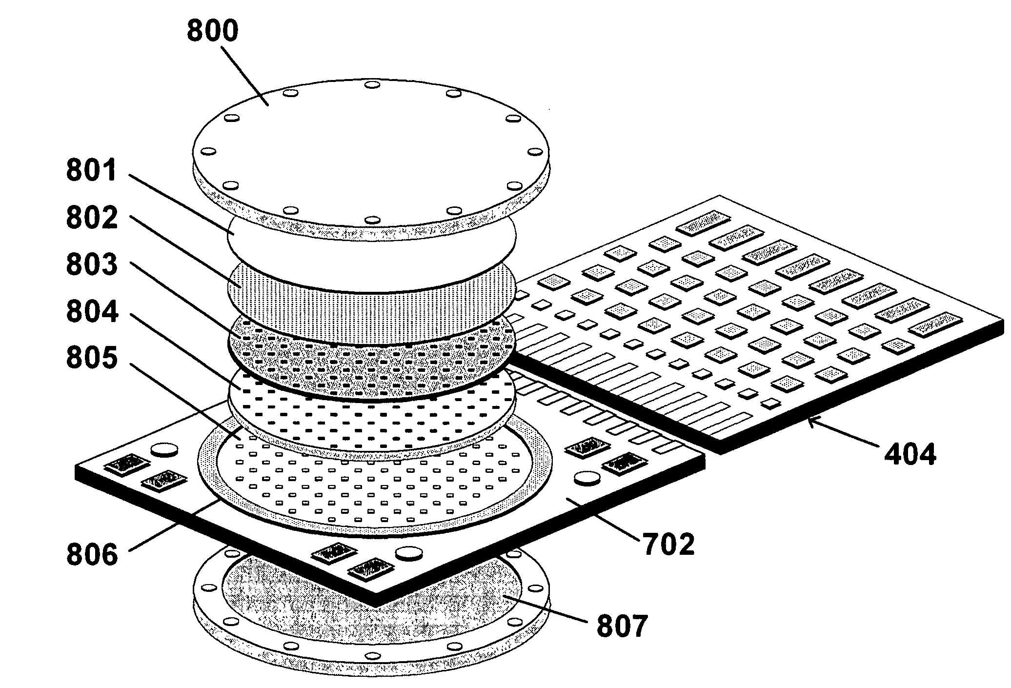
[0018]Various embodiments of the present invention, provide methods and apparatus for conducting burn-in of wafer form, i.e., unsingulated, integrated circuits. These various embodiments are suitable for use with conventional controller boards and conventional burn-in ovens.
[0019]Reference herein to “one embodiment”, “an embodiment”, or similar formulations, means that a particular feature, structure, operation, or characteristic described in connection with the embodiment, is included in at least one embodiment of the present invention. Thus, the appearances of such phrases or formulations herein are not necessarily all referring to the same embodiment. Furthermore, various particular features, structures, operations, or characteristics may be combined in any suitable manner in one or more embodiments.
Terminology
[0020]Reference herein to “circuit boards”, unless otherwise noted, is intended to include any type of substrate upon which circuits may be placed. For example, such substr...
PUM
 Abstract
Description
Claims
Application Information