Apparatus and method for positioning semiconductor substrate

a technology of semiconductor substrates and positioning apparatuses, applied in lighting and heating apparatus, charge manipulation, furnaces, etc., can solve problems such as bending or cracking of wafers, and achieve the effect of safe positioning of wafers

Inactive Publication Date: 2008-12-02
SAMSUNG ELECTRONICS CO LTD
View PDF14 Cites 15 Cited by
  • Summary
  • Abstract
  • Description
  • Claims
  • Application Information

AI Technical Summary

Benefits of technology

[0007]It is, therefore, an object of the present invention to provide an apparat...

Problems solved by technology

This can occur due to malfunctions or positioning errors with respect to the transfer arms.
Such an inclinedly positioned waf...

Method used


Image

  • Apparatus and method for positioning semiconductor substrate
  • Apparatus and method for positioning semiconductor substrate
  • Apparatus and method for positioning semiconductor substrate

Examples


Embodiment Construction

[0028]It should be understood that the description of the preferred embodiment is illustrative and that it should not be taken in a limiting sense. Embodiments of this invention will be explained in conjunction with the drawings.

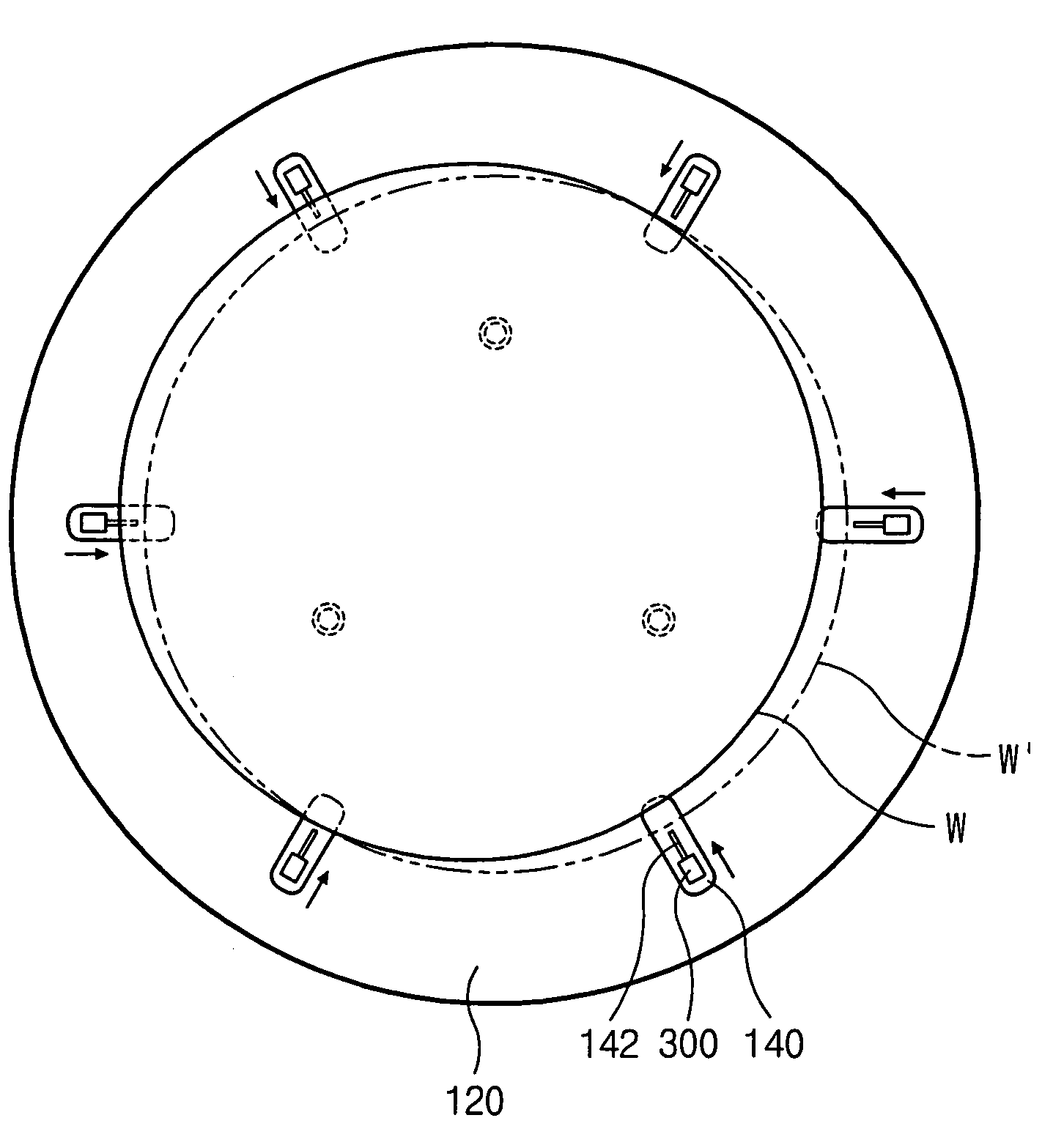
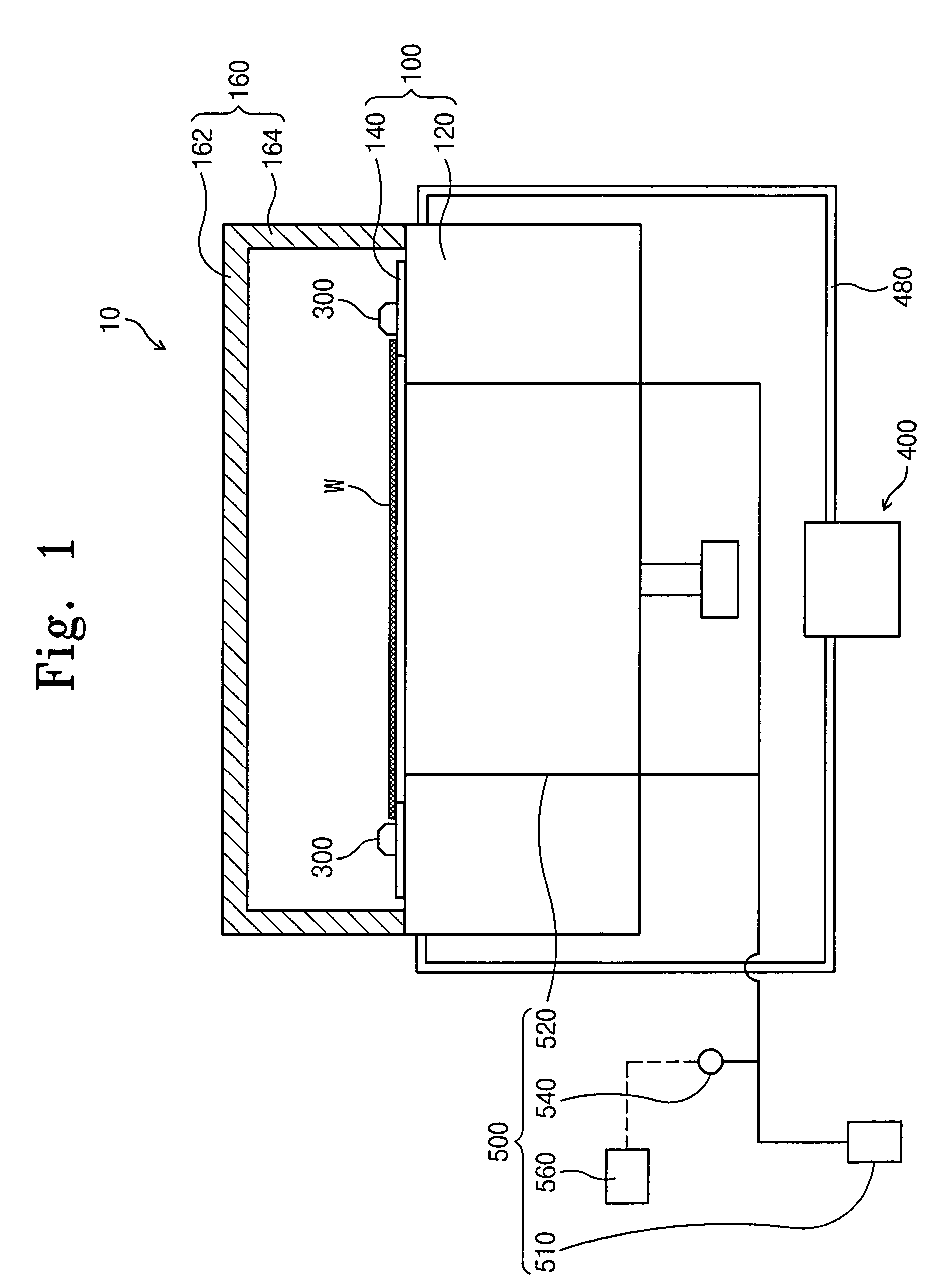
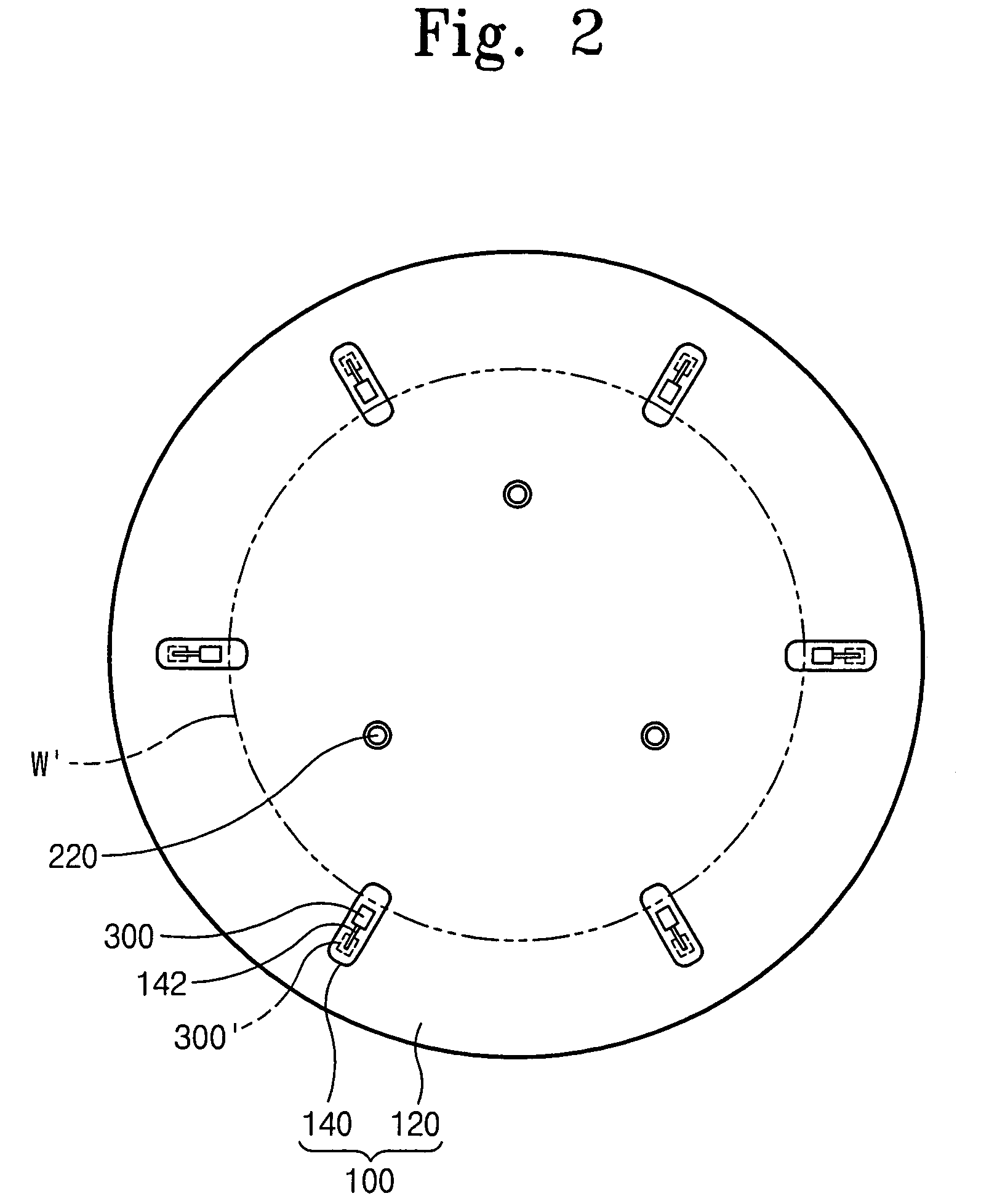
[0029]This preferred embodiment according to the present invention will describe an apparatus and method for carrying out a semiconductor baking process. However, other equipment including a susceptor on which a wafer is mounted may be practiced in accordance with the present invention.

[0030]In this embodiment, “displacement position” of guiding blocks means the position of the guiding blocks during a baking process. “Awaiting position” of the guiding blocks is the position apart from the center of a susceptor, more spaced than the displacement position therefrom, to provide a sufficient margin for loading a wafer on the susceptor. “Normal position” of a wafer means the predetermined position proper to conduct a process (e.g., a baking process). The guiding ...


PUM


Abstract

The disclosure is a baking apparatus including a susceptor, lift pins, and guiding blocks positioned at the edge of the susceptor to lead a wafer to be exactly positioned on the susceptor. The guiding blocks are linearly movable within a range of a semidiameter of a plate. A wafer is partially mounted on a wafer guide, being inclined against the susceptor, and thereby may heats uniformly.

Description

[0001]This application relies for priority upon Korean Patent Application No. 2003-9164 filed on Feb. 13, 2003, and Korean Patent Application No. 2003-47973 filed on Jul. 14, 2003, the contents of which are herein incorporated by reference in their entirety.FIELD OF THE INVENTION[0002]The present invention generally relates to semiconductor manufacturing apparatuses and methods and more specifically, to positioning apparatuses and methods for positioning semiconductor substrates.BACKGROUND OF THE INVENTION[0003]With higher integration densities of semiconductor devices, their chip scales are minimized due to their reduced critical dimensions. These increased integration rates require improved photolithographic technologies for building circuit patterns having finer resolutions. This photolithography technology generally includes the steps of depositing, soft-baking, exposing, hard-baking, and then developing the subject semiconductors devices.[0004]In baking wafers, an apparatus may...

Claims


Application Information

Patent Timeline
IPC IPC(8): B65G49/07H01L21/00H01L21/687
CPCH01L21/67098H01L21/68728H01L21/68742Y10S414/136
Inventor HAN, KWANG-HOKIM, SUN-KYU
Owner SAMSUNG ELECTRONICS CO LTD
Why Eureka
Try Eureka