Method of forming etching mask

a technology of mask and etching, which is applied in the field of forming masks, can solve the problems of mask film b>30/b> not having a desired shape, resists that do not serve as sufficient etching barriers, and mask film eroded,

Inactive Publication Date: 2008-12-16
JUSUNG ENG
View PDF15 Cites 0 Cited by
  • Summary
  • Abstract
  • Description
  • Claims
  • Application Information

AI Technical Summary

Benefits of technology

[0014]Accordingly, the present invention is conceived to solve the aforementioned problems in the prior art. An object of the present invention is to provide a method of forming an etching mask, capable of increasing an etch selectivity of a hard mask film to a photoresist film for forming a fine line width of 193 nm or less, and enhancing an etch rate of the hard mask film.

Problems solved by technology

However, due to the reduction of the line width of a device and the limit of a photolithography process, a thin film pattern with an ultra-fine line width is currently formed using an ArF (193 nm) resist and a hard mask pattern in a line width of 80 nm or less.
This is because the thickness of a resist is reduced due to the limit of a lithography process so that only the existing resist does not serve as a sufficient etch barrier mask.
However, since an etch selectivity of the hard mask film 30 to the photoresist pattern 40 is low when patterning the conventional hard mask film 30 and thus a mask film is eroded, there is a problem in that the pattern of the hard mask film 30 with a desired shape is not formed.
Thus, there is caused a problem in that the photoresist is also removed when the hard mask film 30 is etched, or the durability of the photoresist is weakened by the mixed gas when etching the hard mask film 30 having the same thickness as the photoresist and the photoresist is collapsed.
Thereafter, in a case where the thin film 20 is patterned by performing an etching process using the pattern of the hard mask film 30 with the aforementioned large width as an etching mask, there is caused a problem in that a thin film pattern with a width larger than that of an initially desired shape is formed.
Accordingly, there is caused a problem in that the lower hard mask film 30 is not patterned, and thus it is impossible to pattern the thin film 20.

Method used


Image

  • Method of forming etching mask
  • Method of forming etching mask
  • Method of forming etching mask

Examples


Embodiment Construction

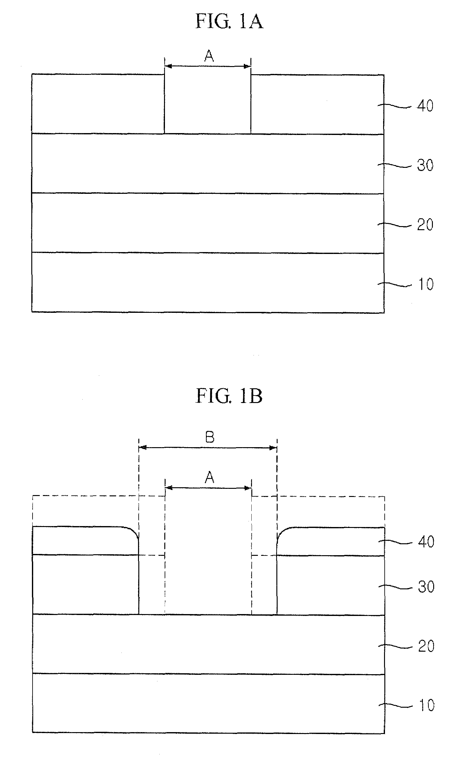
[0037]Hereinafter, preferred embodiments of the present invention will be described in detail with reference to the accompanying drawings. However, the present invention is not limited to the embodiments to be disclosed below but may be implemented into a variety of different forms. The embodiments are provided only for illustrative purposes and for full understanding of the scope of the present invention to those skilled in the art. Throughout the drawings, like elements are designated by like reference numerals.

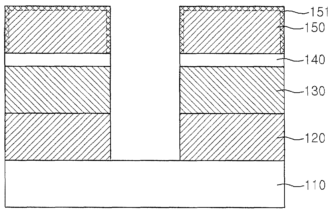
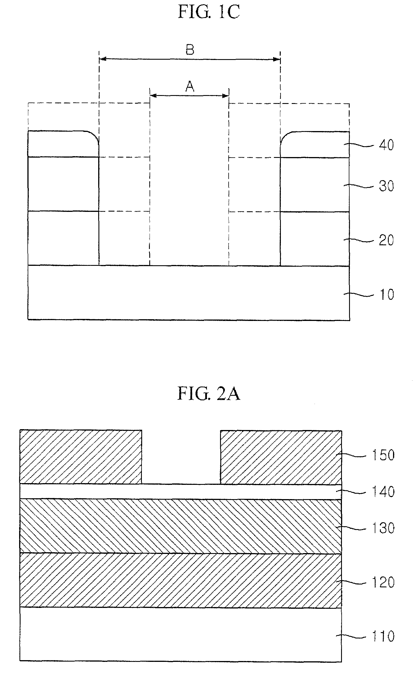
[0038]FIGS. 2A to 2D are sectional views illustrating a method of forming a thin film pattern according to the embodiment of the present invention.

[0039]As shown in FIG. 2A, a thin film 120, a hard mask film 130 and a anti reflective coating (ARC) 140 are formed on a substrate 110. Thereafter, photoresist is applied to the ARC 140, and a photoresist pattern 150 is then formed by performing a lithography process using a mask.

[0040]Here, as the substrate 110, not only a semic...


PUM

PropertyMeasurementUnit
widthaaaaaaaaaa
thicknessaaaaaaaaaa
wavelengthaaaaaaaaaa

Abstract

The present invention relates to a method of forming an etching mask. According to the present invention, there is provided a method of forming an etching mask, comprising the steps of: depositing a hard mask film containing silicon on a substrate; depositing a photoresist on the hard mask film; patterning the photoresist; and etching the hard mask film using the photoresist pattern as an mask and using an etching gas including a CHxFy(x, y=1, 2, 3) gas. At this time, an etch selectivity of the hard mask film to the photoresist pattern can be increased using a mixed gas including CH2F2 and H2 gases when etching the hard mask film under the photoresist pattern used in a wavelength of 193 nm or less.

Description

CROSS-REFERENCE TO RELATED APPLICATIONS[0001]This U.S. non-provisional patent application claims priority under 35 U.S.C. § 119 of Korean Patent Applications 2005-0104528 filed on Nov. 2, 2005, the entire contents of which are hereby incorporated by reference.BACKGROUND OF THE INVENTION[0002]1. Field of Invention[0003]The present invention relates to a method of forming an etching mask, and more particularly, to a method of forming an etching mask with a high etch selectivity of a hard mask for forming a thin film pattern to a photoresist.[0004]2. Description of the Prior Art[0005]Conventionally, in order to form a thin film pattern, a G-line (436 nm) resist and an I-line (365 nm) resist or a KrF (248 nm) resist are applied, and a photoresist pattern is then formed by performing a photolithography process using a mask. Thereafter, a thin film pattern is formed by performing an etching process using the photoresist pattern as an etching mask.[0006]However, due to the reduction of the...

Claims


Application Information

Patent Timeline
Patent Type & Authority Patents(United States)
IPC IPC(8): H01L21/302
CPCG03F7/11G03F7/40G03F7/405H01L21/0273H01L21/32139H01L21/3081H01L21/3086H01L21/31116H01L21/31144H01L21/0337
Inventor KWON, GI-CHUNGLEE, NAE-EUNGPARK, CHANG-KILEE, CHUN-HEEKIM, DUCK-HO
Owner JUSUNG ENG
Why Eureka
Try Eureka