

Flash memory device and method of manufacturing the same
a flash memory and manufacturing method technology, applied in the direction of semiconductor devices, electrical devices, transistors, etc., can solve the problems of interference phenomenon, interference phenomenon, narrow inter-gate distance, etc., to reduce cell leakage, reduce disturb effect, and minimize threshold voltage
- Summary
- Abstract
- Description
- Claims
- Application Information
AI Technical Summary
Benefits of technology
Problems solved by technology
Method used
Image

Examples
first embodiment
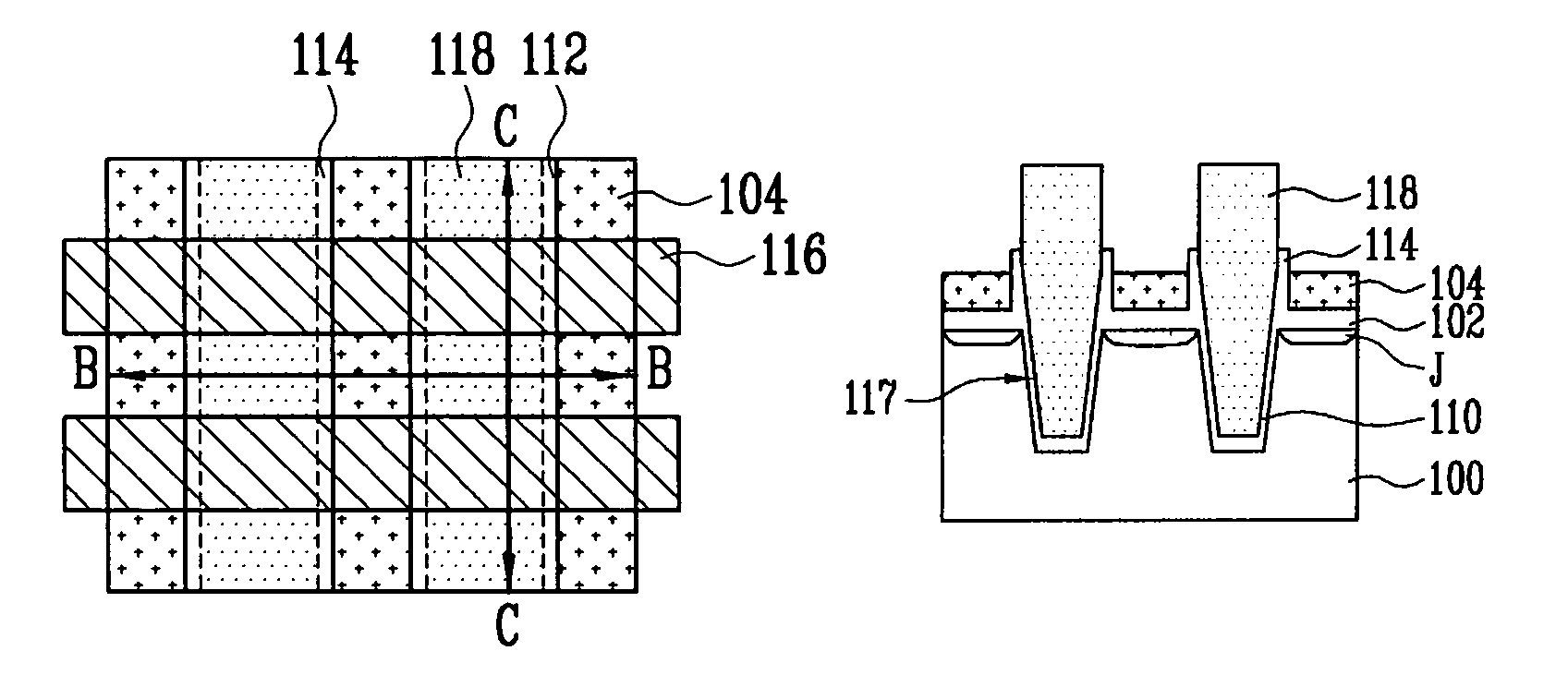
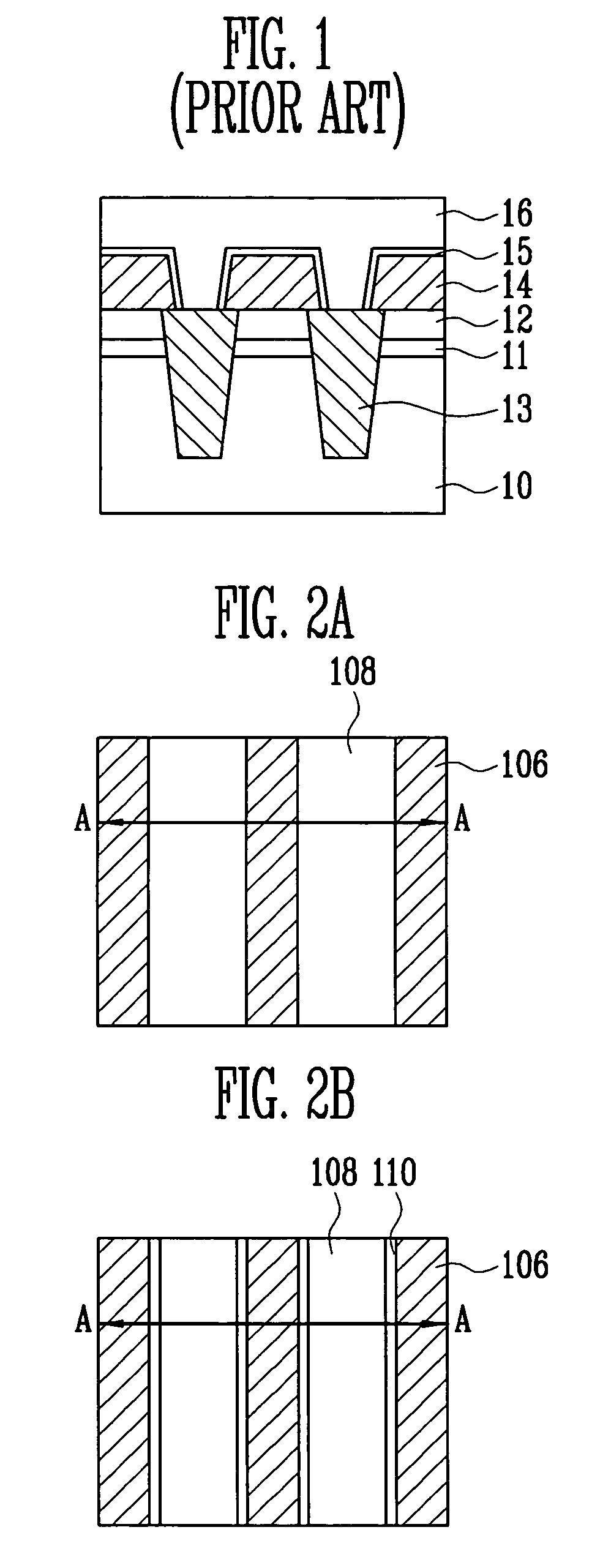
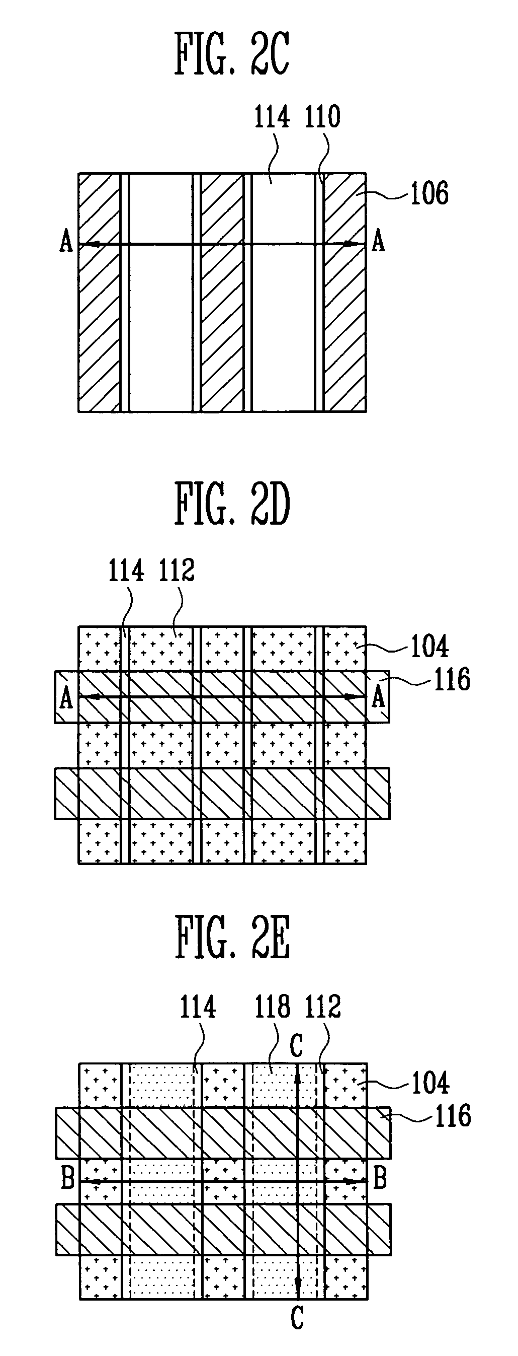
[0019]FIGS. 2A to 2E are layout diagrams illustrating a flash memory device to which a self-aligned STI is applied according to the present invention. FIGS. 3A to 3F are cross-sectional views of the flash memory devices corresponding to the layout diagrams of FIGS. 2A to 2E, respectively.
[0020]FIG. 3A is a cross-sectional view of the flash memory device taken along line A-A in FIG. 2A. Referring to FIGS. 2A and 3A, a high concentration ion implantation process is performed to form a junction unit J on a semiconductor substrate 100. A first oxide film 102 is thickly formed on the semiconductor substrate 100. Since a high concentration of ions has been injected into the semiconductor substrate 100, the first oxide film 102 can be thickly formed using a low thermal process. The first oxide film 102 may be formed to a thickness of about 300 Å to about 500 Å.
[0021]A first polysilicon film 104 and a hard mask film 106 are sequentially formed on the first oxide film 102. The hard mask film...
second embodiment
[0038]FIGS. 4A to 4D are layout diagrams illustrating a flash memory device to which a general STI is applied according to the present invention. FIGS. 5A to 5E are cross-sectional views of the flash memory devices corresponding to the layout diagrams of FIGS. 4A to 4D, respectively.
[0039]FIG. 5A is a cross-sectional view of the flash memory device taken along line D-D in FIG. 4A.
[0040]Referring to FIGS. 4A and 5A, a high concentration ion implantation process is performed to form junction units J on a semiconductor substrate 200. A first oxide film 202 is thickly formed on the semiconductor substrate 200. Since the ion of a high concentration has been injected into the semiconductor substrate 200, the first oxide film 202 can be formed thickly even using a low thermal process. The first oxide film 202 may be formed to a thickness of about 300 Å to about 500 Å.
[0041]The first oxide film 202 and the semiconductor substrate 200 are selectively etched by photolithography and etch proce...
PUM
 Abstract
Description
Claims
Application Information