Substrate structure having a solder mask and a process for making the same

a technology of solder mask and packaging structure, which is applied in the direction of resisting details, printed circuit manufacturing, patterning and lithography, etc., can solve the problems of polluting the solder mask b>103/b>, and achieve the effect of preventing the die crack

Active Publication Date: 2009-01-06
ADVANCED SEMICON ENG INC
View PDF6 Cites 30 Cited by
  • Summary
  • Abstract
  • Description
  • Claims
  • Application Information

AI Technical Summary

Benefits of technology

[0010]The solder mask of the above-mentioned structure of the invention is a single structure. By utilizing the higher second portion of the solder mask, a thicker die can be used to be packaged so as to prevent the die crack. Furthermore, the second portion is stair-shaped, and a ring-shaped groove also can be formed on the second portion, so that the overflow of molding compound will be avoided, and the solder pads will not be polluted.
[0012]The solder mask of the above-mentioned structure of the invention is a delaminated structure. Since the second solder mask is formed on part of the first solder mask to form a higher solder mask, a thicker die can be used to be packaged so as to prevent the die crack. Furthermore, the first solder mask and the second solder mask form a stair-shaped structure, and a ring-shaped groove may be formed on the second solder mask. Therefore, the overflow of molding compound will be avoided, and the solder pads will not be polluted.

Problems solved by technology

Furthermore, the solder mask 11 cannot avoid the overflow of molding compound so that the solder pads 103 will be polluted.

Method used


Image

  • Substrate structure having a solder mask and a process for making the same
  • Substrate structure having a solder mask and a process for making the same
  • Substrate structure having a solder mask and a process for making the same

Examples


Embodiment Construction

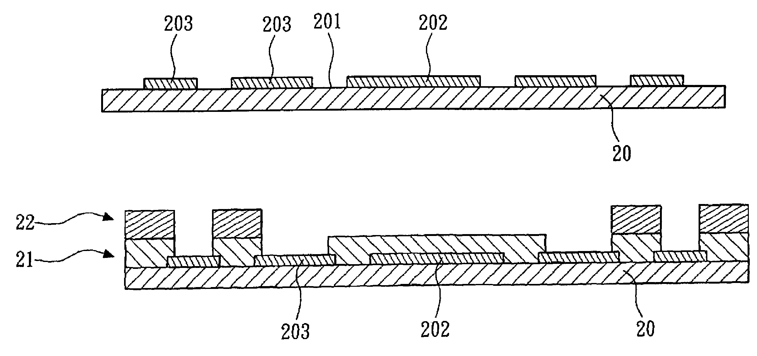
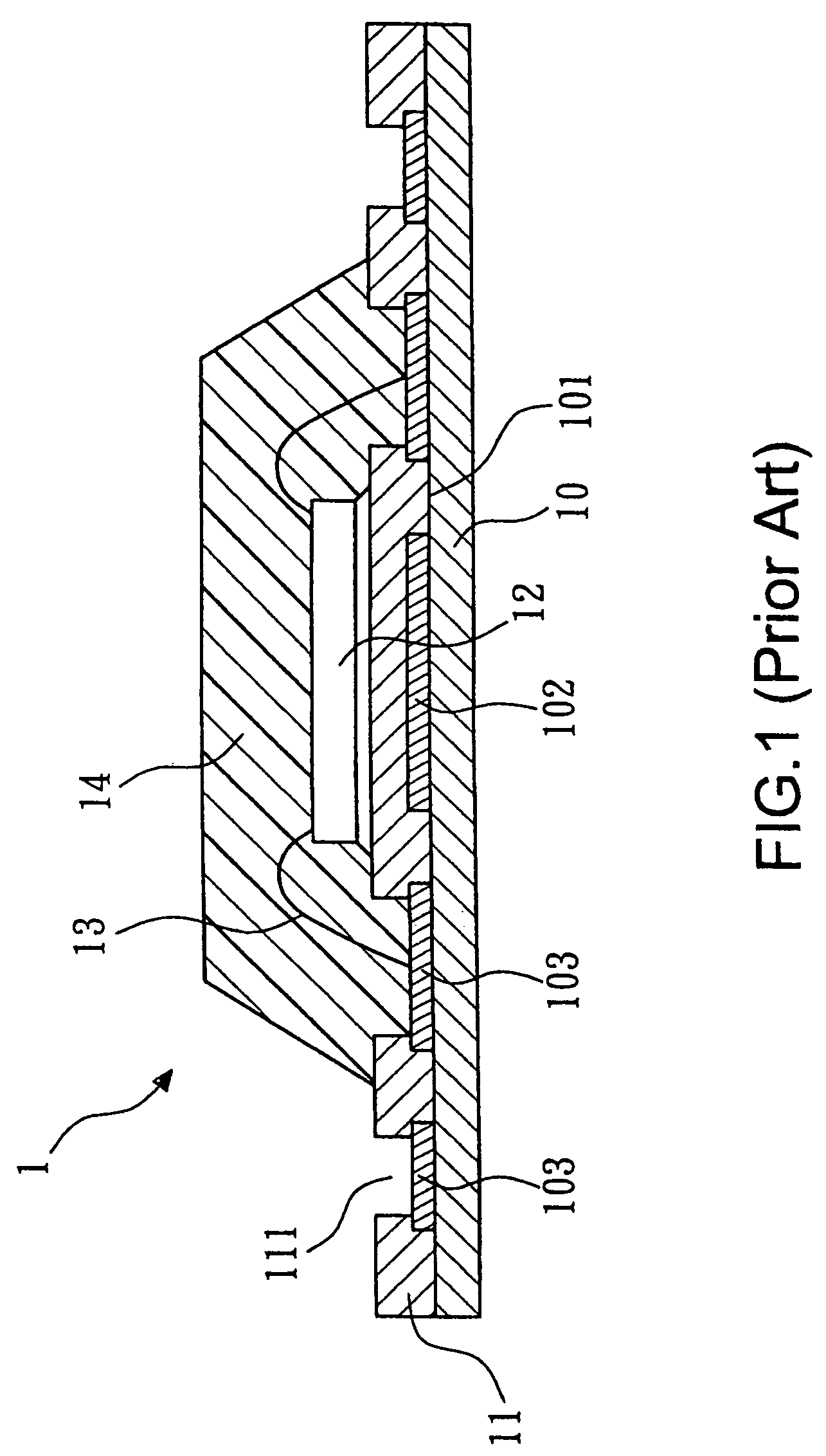
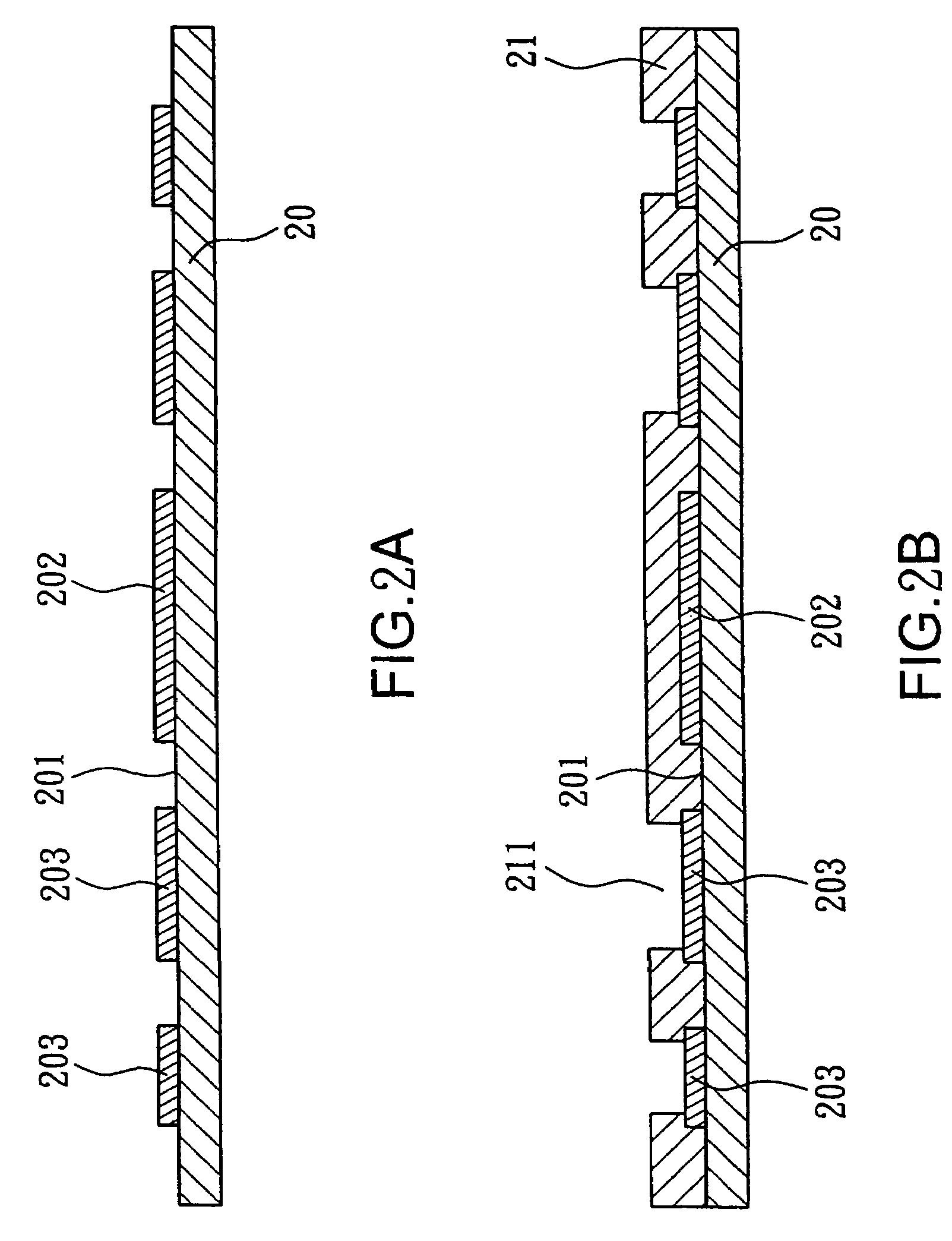
[0019]Referring to FIGS. 2A to 2D, they show the processes for making a substrate structure having a solder mask according to the present invention. Referring to FIG. 2A, firstly, a substrate 20 is provided. The substrate 20 has a top surface 201, and the top surface 201 has a die pad 202 and a plurality of solder pads 203. Referring to FIG. 2B, a first solder mask 21 is formed on the top surface 201. The first solder mask 21 has a plurality of openings 211. Each opening 211 is corresponding to each solder pad 203 so as to expose the solder pad 203. In the embodiment, the openings 211 are formed by using exposure and development.

[0020]Referring to FIG. 2C, a second solder mask 22 is formed on the first solder mask 21 and the solder pads 203. Referring to FIG. 2D, part of the second solder mask 22 is then removed by using exposure and development so as to expose part of the solder pads 203 and the first solder mask 21. The exposed part of the first solder mask 21 is corresponding to ...


PUM

PropertyMeasurementUnit
heightaaaaaaaaaa
structureaaaaaaaaaa
widthaaaaaaaaaa

Abstract

A substrate structure having a solder mask and a process for making the same, including (a) providing a substrate having a top surface, the top surface having a die pad and a plurality of solder pads; (b) forming a first solder mask on the top surface, the first solder mask having a plurality of openings, each opening corresponding to each solder pad so as to expose at least part of the solder pad; and (c) forming a second solder mask on the first solder mask. The substrate structure can be used for packaging a thicker die so as to prevent the die crack and the overflow of molding compound will be avoided.

Description

BACKGROUND OF THE INVENTION[0001]1. Field of the Invention[0002]The invention relates to a substrate structure and a process for making the same, particularly to a packaging structure having a solder mask and a process for making the same.[0003]2. Description of the Related Art[0004]Referring to FIG. 1, it shows a conventional substrate structure. The structure 1 of the invention comprises a substrate 10, a solder mask 11, a die 12, a plurality of wires 13 and molding compound 14. The substrate 10 has a top surface 101. The top surface 101 has a die pad 102 and a plurality of solder pads 103. The solder mask 11 is formed on the top surface 101. The solder mask 11 has a plurality of openings 111. The openings 111 are formed by using exposure and development. Each opening 111 is corresponding to each solder pad 103 to expose part of the solder pad 103.[0005]The die 12 is attached on the solder mask 11 correspondingly on the die pad 102. The wires 13 are used to electrically connect th...

Claims


Application Information

Patent Timeline
Patent Type & Authority Patents(United States)
IPC IPC(8): H01L21/44
CPCH05K3/3452H05K3/284H05K2203/0588H01L2224/32225H01L2224/48091H01L2224/48227H01L2224/48228H01L2224/73265H01L2924/00014H01L2924/00
Inventor TAI, WEI-CHANGCHU, CHI-CHIHCHUANG, MENG-JUNGLEE, CHENG-YINHUANG, YAO-TINGLO, KUANG-LIN
Owner ADVANCED SEMICON ENG INC
Why Eureka
Try Eureka