

Apparatus and methods for constructing and packaging waveguide to planar transmission line transitions for millimeter wave applications
a technology of waveguides and transitions, applied in electrical apparatus, waveguides, coupling devices, etc., can solve the problems of increased losses at high frequencies, printed transmission lines may be subject to parasitic modes, etc., and achieve high-performance coupling power
- Summary
- Abstract
- Description
- Claims
- Application Information
AI Technical Summary
Benefits of technology
Problems solved by technology
Method used
Image

Examples
Embodiment Construction
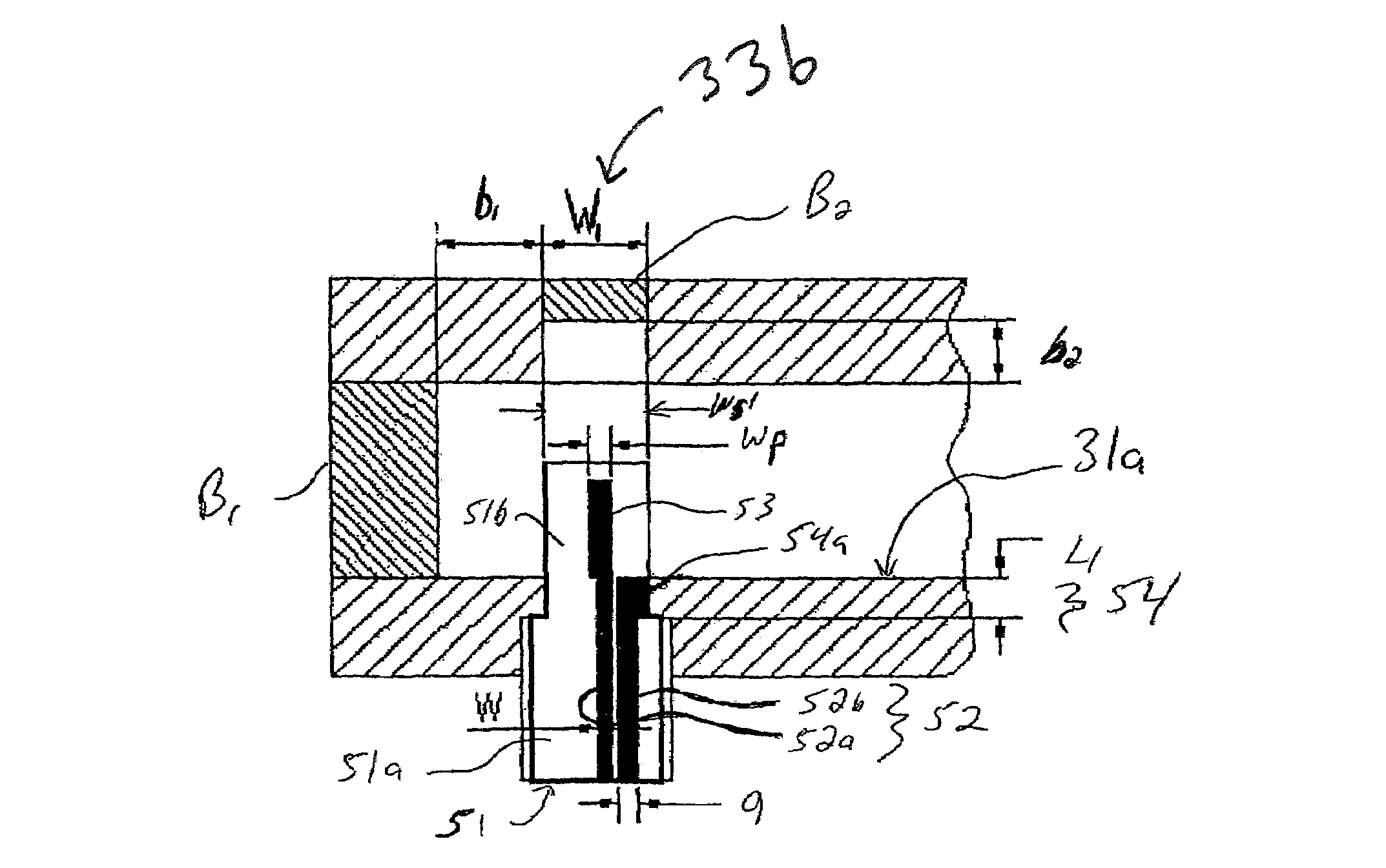
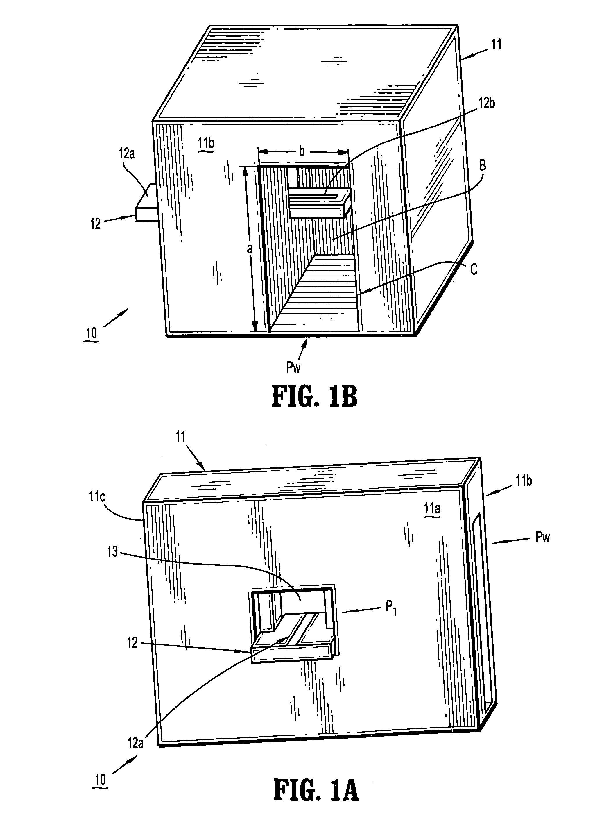
[0023]FIGS. 1A and 1B are schematic perspective views of a transmission line to waveguide transition apparatus (10) according to an exemplary embodiment of the invention. More specifically, FIGS. 1A and 1B schematically depict a transition apparatus (10) for coupling electromagnetic signals between a rectangular waveguide (e.g., WR15) and a printed transmission line using an E-plane probe-type transition, according to an exemplary embodiment of the invention. The transition apparatus (10) comprises a metallic transition housing (11) (or waveguide block) which has an inner rectangular waveguide cavity C (or rectangular waveguide channel) of width a (broad wall) and height b (short wall). An aperture (13) is formed in a front wall (11a) of the waveguide block (11) through a broad wall of the rectangular waveguide cavity C to provide a transition port PT for insertion and support of a planar transition substrate (12) having a printed transmission line (12a) and printed E-plane probe (1...
PUM
 Abstract
Description
Claims
Application Information