[0012] These and other exemplary embodiments, aspects, features and advantages of the present invention will be described or become apparent from the following detailed description of exemplary embodiments, which is to be read in connection with the accompanying drawings.
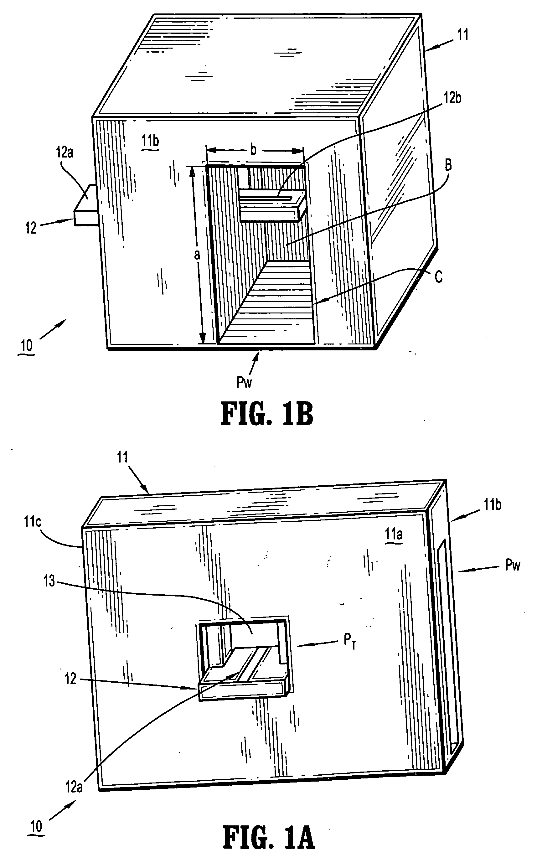
[0013]FIGS. 1A and 1B are
schematic perspective views of a transmission line to waveguide transition apparatus (10) according to an exemplary embodiment of the invention.
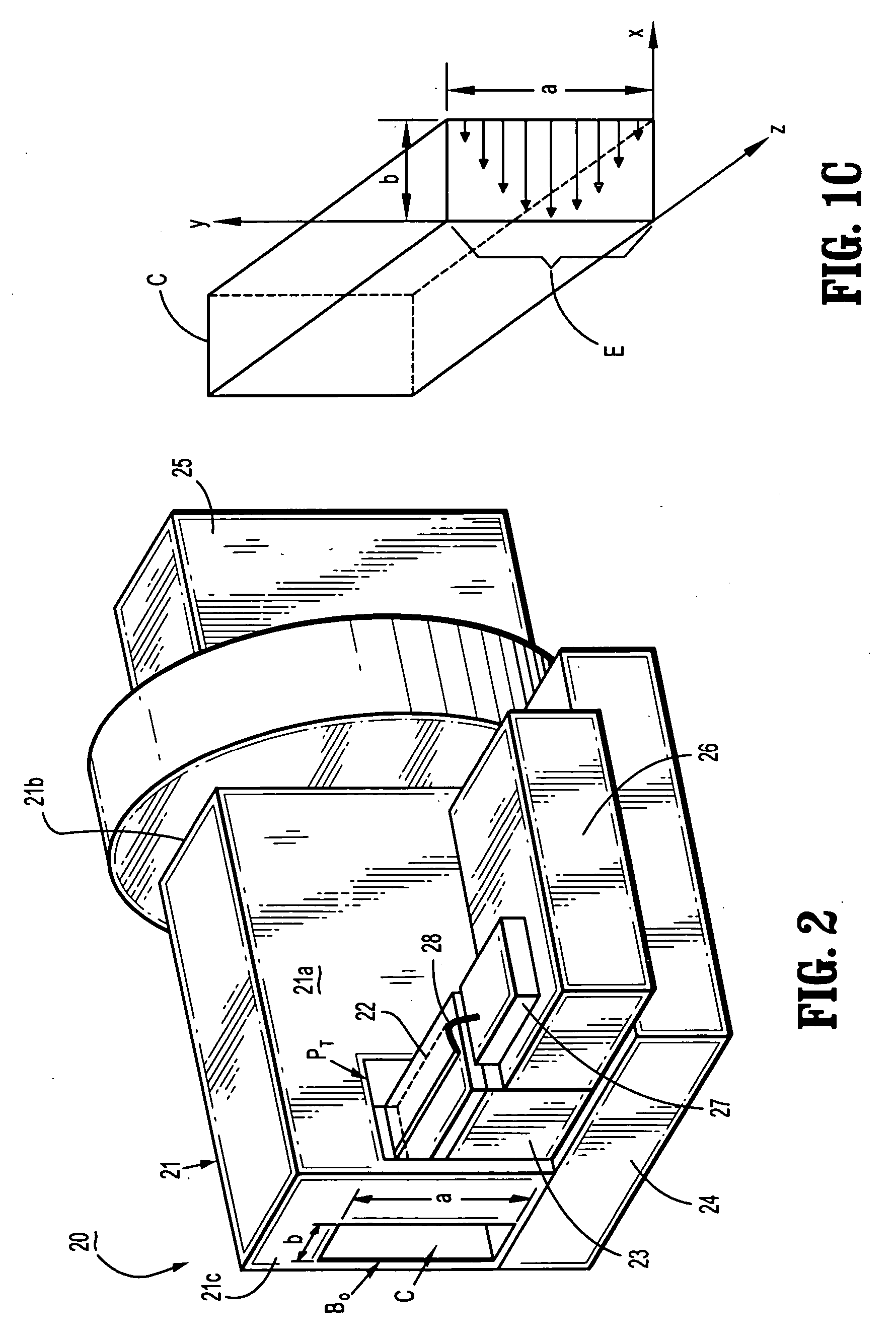
[0014]FIG. 1C is a
schematic illustration of the rectangular waveguide cavity C illustrating a dominant TE10 propagation mode.
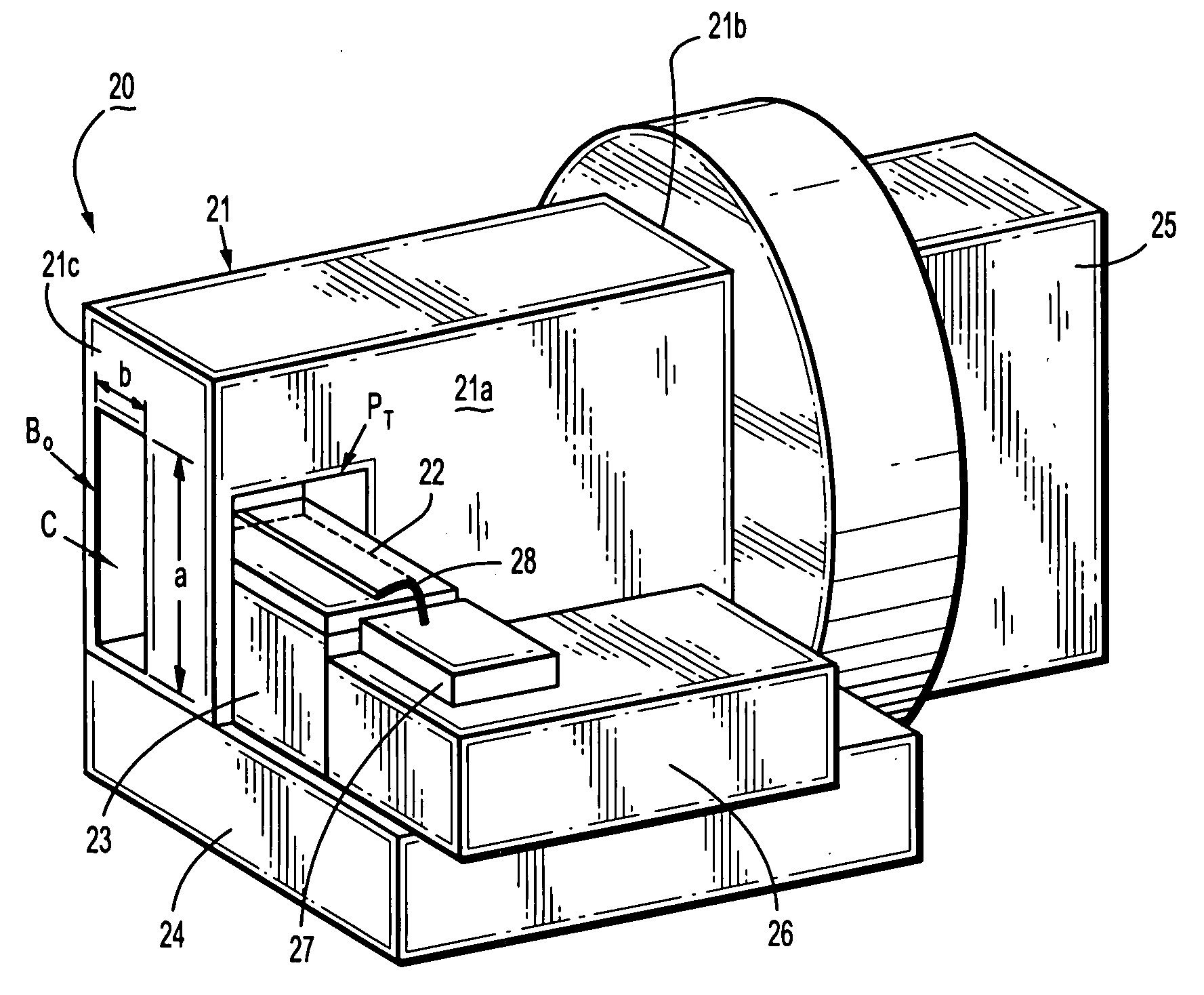
[0015]FIG. 2 is a
schematic perspective view of a
package assembly (20) including a transmission line-to-waveguide transition module that is integrally packaged with external circuitry according to an exemplary embodiment of the invention.
[0016] FIGS. 3A˜3D illustrate structural details of a metallic transition housing (30) according to an exemplary embodiment of the invention
[0017] FIGS. 4A˜4C are schematic perspective views of a transmission line to waveguide transition apparatus according to an exemplary embodiment of the invention.
[0018] FIGS. 5A˜5C are schematic perspective views of a transmission line to waveguide transition apparatus according to an exemplary embodiment of the invention.
[0019]FIG. 6 schematically illustrates a conductor-backed CPW feed structure in which half-via edge wrapping metallization is used for suppressing undesired waveguide
modes and resonances, according to an exemplary embodiment of the invention.
[0020]FIG. 7 schematically illustrates a non conductor-backed CPW feed structure in which half-via edge wrapping metallization is used for suppressing undesired waveguide
modes and resonances, according to an exemplary embodiment of the invention.
[0021]FIG. 8 schematically illustrates a conductor-backed CPS feed structure in which half-via edge wrapping metallization is used for suppressing undesired waveguide modes and resonances, according to an exemplary embodiment of the invention.
[0022]FIG. 9 schematically illustrates a non-conductor-backed CPS feed structure in which half-via edge wrapping metallization is used for suppressing undesired waveguide modes and resonances, according to an exemplary embodiment of the invention.
[0023]FIGS. 1A and 1B are schematic perspective views of a transmission line to waveguide transition apparatus (10) according to an exemplary embodiment of the invention. More specifically, FIGS. 1A and 1B schematically depict a transition apparatus (10) for
coupling electromagnetic signals between a rectangular waveguide (e.g., WR15) and a printed transmission line using an E-plane probe-type transition, according to an exemplary embodiment of the invention. The transition apparatus (10) comprises a metallic transition housing (11) (or waveguide block) which has an inner rectangular waveguide cavity C (or rectangular
waveguide channel) of width a (broad wall) and height b (short wall). An aperture (13) is formed in a front wall (11a) of the waveguide block (11) through a broad wall of the rectangular waveguide cavity C to provide a transition port PT for
insertion and support of a planar transition substrate (12) having a printed transmission line (12a) and printed E-plane probe (12b). The transition substrate (12) is positioned in the aperture (13) such that the probe (12b) protrudes into the waveguide cavity C through the broad wall of waveguide cavity C. One end of the waveguide cavity C is opened on a side wall (11b) of the transition housing (11) to provide a waveguide input port Pw, The other end of the waveguide cavity C is short-circuited by sidewall (11c) of the transition housing (11), whereby the inner surface of the metallic sidewall (11c) serves as a backshort B for the probe (12b).
[0024] In one exemplary embodiment of the invention, the probe (12b) is an E-plane type probe which is designed to sample the
electric field within the rectangular waveguide cavity C where the rectangular waveguide is operated in the dominant TE10 mode. As is well-known in the art, in a rectangular waveguide, the
electric field is normal to the broad sidewall and the
magnetic field line is normal to the short sidewall. By way of example, FIG. 1C is a schematic illustration of the rectangular waveguide cavity C where the short sidewalls (b) extend in the x-direction (coplanar with x-z plane), the broad sidewalls (a) extend in the y-direction (coplanar with y-z plane), and where the cavity C extends in the z-direction (i.e., the direction of
wave propagation along the
waveguide channel). FIG. 1C further illustrates an E field for the TE10 mode is in the x-y plane (normal to the broad walls) where the maximum positive and
negative voltage peaks of the TE wave travel down the center of the waveguide broad walls (a) and the
voltage decreases to zero along the waveguide short walls (b).
[0025] In this regard, in the exemplary embodiment of FIGS. 1A and 1B, the substrate (12) with the printed probe (12b) is inserted through the transition port PT in the broad sidewall (11a) such that the probe (12b) is positioned transverse (normal) to the direction of
wave propagation (i.e., z-direction in FIG. 1C) and such that the plane of substrate (12) is positioned tangential to the direction of
wave propagation (i.e., plane of substrate (12) is coplanar with x-z plane in FIG. 1C). The sidewall (11c) of the
metal block (11) serves as a backshort B such that the inner surface of the side wall (11c) is placed in a certain distance (close to a quarter-
wavelength for TE10 mode) behind the probe (12b) to achieve good
transmission properties.
[0026] It is to be understood that FIGS. 1A and 1B schematically depict a general framework for a waveguide-to-planar transmission line transition apparatus according to an embodiment of the invention. The printed E-plane probe (12b) may have any suitable shape and configuration which is designed to sample the
electric field within the rectangular waveguide cavity C. The printed transmission line (12a) may be any suitable feed structure such as a printed CPW (coplanar wave guide) feed, ACPS (asymmetric coplanar
stripline) feed, or CPS (coplanar
stripline) feed. For example, as described in further detail below, FIGS. 4A˜4C, 5A˜5C and 6˜9 illustrate transition structures according to various exemplary embodiments of the invention, which may be constructed with transition substrates having printed conductor-backed and non-conductor backed CPW and CPS feed lines and planar probe transitions, as will be explained in further detail below.
[0027] In other exemplary embodiments of the invention, the exemplary transition structure of FIGS. 1A˜1B can be integrally packaged with electronic components, such as MIC or MMIC modules to construct compact
package structures. For instance, FIG. 2 is a schematic perspective view of a
package assembly (20) including a transmission line-to-waveguide transition module that is integrally packaged with external circuitry according to an exemplary embodiment of the invention. The exemplary package (20) includes a transition housing (21) (or waveguide block) having an inner rectangular
waveguide channel C. The transition housing (21) has a front wall (21a) with an aperture extending through a broad wall of the inner rectangular waveguide channel C providing a transition port PT. A transition substrate (22) with a printed transmission line and E-plane probe is inserted into the waveguide cavity through the transition port PT.


