Display device

a display device and display technology, applied in semiconductor devices, transistors, instruments, etc., can solve the problems of increasing achieve the effect of reducing cost and power consumption, improving gray scale reproducibility and color reproducibility, and improving color reproducibility

Inactive Publication Date: 2009-02-17
SEMICON ENERGY LAB CO LTD
View PDF1 Cites 7 Cited by
  • Summary
  • Abstract
  • Description
  • Claims
  • Application Information

AI Technical Summary

Benefits of technology

[0009]In that case, it is necessary to provide a power source for each color, and thus an external circuit is increased, leading to increase in the cost and power consumption. In view of the foregoing problems, the invention provides a display device of which an external circuit is made smaller and the cost and power consumption are reduced.
[0013]Accordingly, when a signal voltage applied to a control gate of a VS-MOS is controlled for each sub-pixel, the amount of current or the current density flowing in a light emitting element can be controlled, and thereby luminance can be controlled for each sub-pixel.
[0016]According to the invention having the structure described above, a display device of which an external circuit is made smaller and the cost and power consumption are reduced can be provided as well as a manufacturing method thereof. In addition, the invention can provide a display device of which gray scale reproducibility and color reproducibility are improved as well as a manufacturing method thereof.

Problems solved by technology

In that case, it is necessary to provide a power source for each color, and thus an external circuit is increased, leading to increase in the cost and power consumption.

Method used


Image

  • Display device
  • Display device
  • Display device

Examples


embodiment mode 1

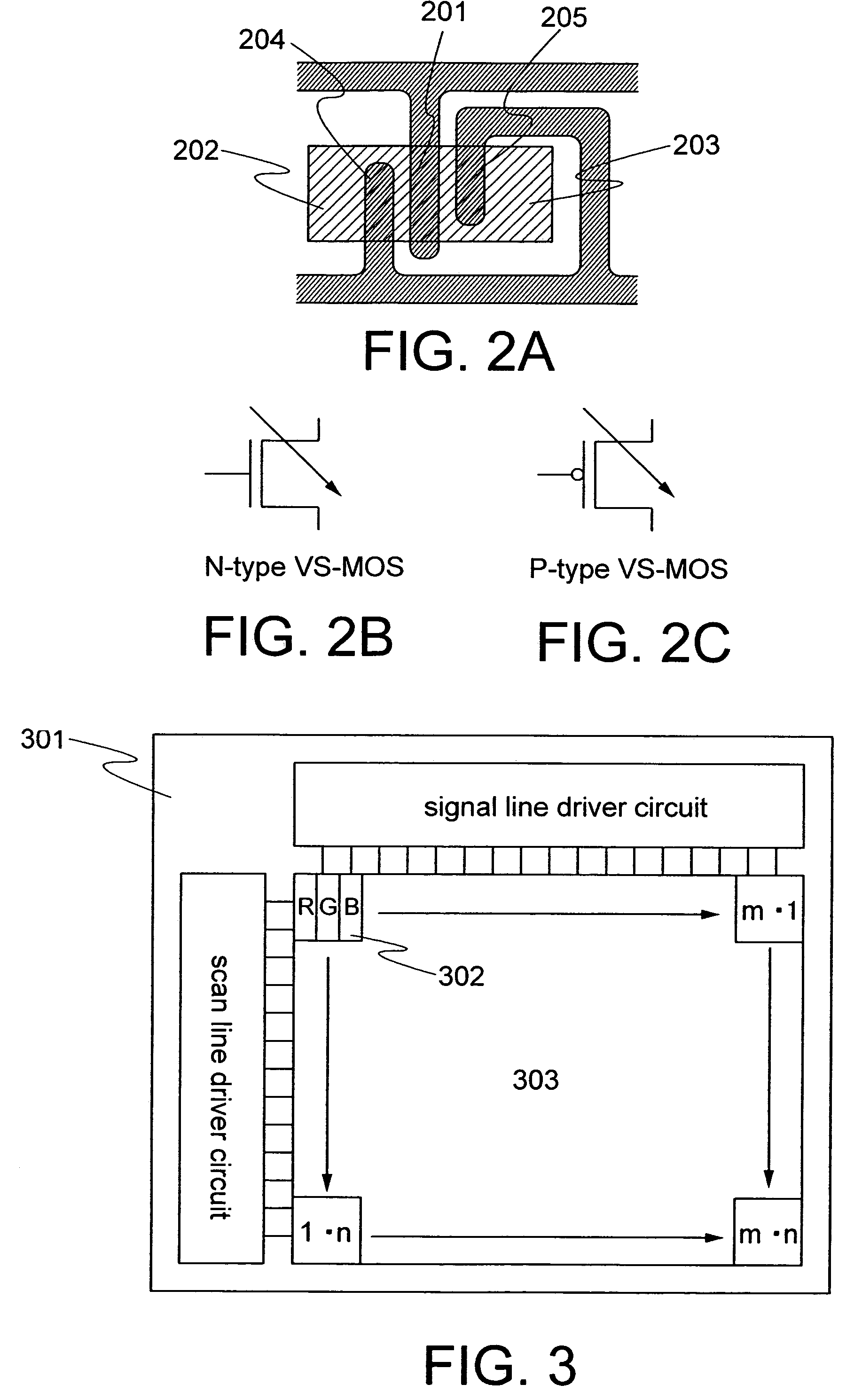
[0030]First, an example of a schematic layout of a VS-MOS and circuit symbols are shown in FIGS. 2A to 2C. As shown in the drawings, a VS-MOS comprises a control gate 204 between a main gate 201 and a source region 202, and a control gate 205 between the main gate 201 and a drain region 203. In the VS-MOS having such a structure, when varying a voltage applied to the control gates 204 and 205, it is possible to change a current value flowing between the source region 202 and the drain region 203 without varying a voltage applied to the main gate 201.

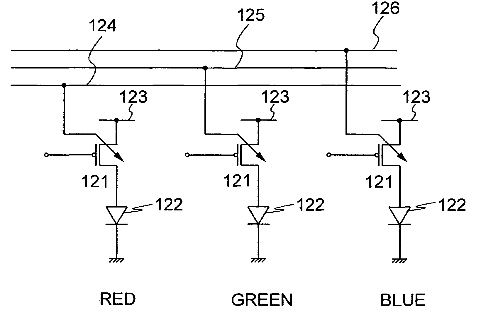
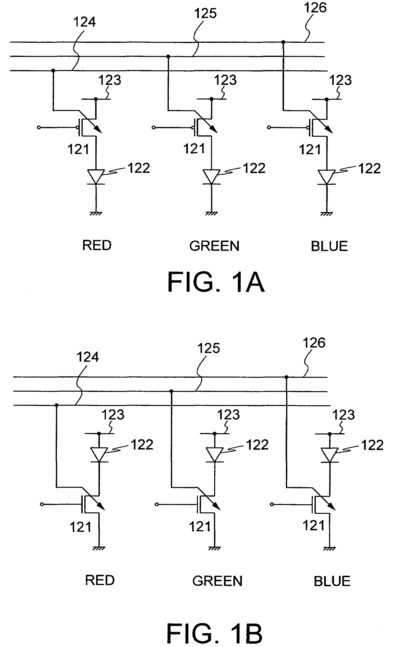
[0031]Next, shown in FIG. 3 is a structure of a display device in which the VS-MOS is used for a transistor for driving a light emitting element. A display device comprises over a substrate 301 a pixel portion 303 that includes m×n pixels 302 arranged in matrix. Each of the pixels 302 includes three sub-pixels each corresponding to one of RGB. It is noted that the sub-pixels correspond to the ones formed of light emitting elements using ...

embodiment mode 2

[0037]In the invention, a transistor obtained in manufacturing steps described below can be employed. Described hereinafter are manufacturing steps of a VS-MOS.

[0038]A droplet ejection method here means a method typified by an inkjet method and a dispenser method.

[0039]A composition containing a conductive material is ejected onto a substrate 401 by the droplet ejection method to form a conductive layer 402 functioning as a gate electrode and conductive layers 403 functioning as control gates (see FIG. 4A).

[0040]Then, an insulating layer 404 functioning as an insulating film is formed. The insulating layer 404 may be formed of a single layer or a plurality of stacked layers. Further, an I-type amorphous silicon layer 405 and an N-type amorphous silicon layer 406 are formed. Subsequently, the I-type amorphous silicon layer 405 and the N-type amorphous silicon layer 406 are patterned using a resist or the like used as a mask, then the resist or the like used as a mask is removed (see ...

embodiment mode 3

[0047]A pixel circuit using the invention is described with reference to FIGS. 6A and 6B. FIG. 6A shows an area surrounded by a signal line 6114, power source lines 6115 and 6117, and a scan line 6116, which includes a transistor 6110 for controlling a video signal input to a pixel 6101, a transistor 6111 for controlling a current value flowing into a light emitting element 6113, a control gate signal line 6100 for supplying a signal to a control gate of the transistor 6111, and a capacitor 6112 for holding a gate-source voltage of the transistor 6111. It is noted that a gate capacitance or other parasitic capacitance of the transistor 6111 may be used instead of the capacitor 6112.

[0048]FIG. 6B shows a pixel circuit in which a transistor 6118 and a scan line 6119 are additionally provided in the pixel 6101 shown in FIG. 6A. The transistor 6118 makes a state in which a current supply to the light emitting element 6113 is forcibly stopped. Therefore, a lighting time can be started si...


PUM


Abstract

In a conventional display device using light emitting elements, white color cannot be accurately displayed since the luminance of each sub-pixel varies for each color. Therefore, in order to achieve the uniformity in luminance of each sub-pixel, the amount of current or the current density flowing in light emitting elements is required to be changed for each color. In that case, a power source is necessarily provided for each color, thus an external circuit is increased, leading to increase in the cost and power consumption. According to the invention, a variable channel-size MOS transistor is used as a transistor for driving a light emitting element. When a signal voltage applied to a control gate is controlled for each sub-pixel, the amount of current or the current density flowing in light emitting elements can be adjusted and luminance of each sub-pixel can also be adjusted for each color.

Description

BACKGROUND OF THE INVENTION[0001]1. Field of the Invention[0002]The present invention relates to a display device using light emitting elements and a manufacturing method thereof. More particularly, the invention relates to a multicolor display device and a manufacturing method thereof.[0003]2. Description of the Related Art[0004]In recent years, the development of a display device using light emitting elements has been advanced. A display device that is currently under development is the one in which one pixel is divided into three sub-pixels each corresponding to one of R (Red), G (Green) and B (Blue) that are the three primary colors of light, and a gray scale display is performed in each of the sub-pixels for RGB, and thereby performing a multicolor display. When performing the multicolor display, typically, light emitting elements are formed by using light emitting materials corresponding to RGB, or a light emitting element that emits white light is used in combination with RGB...

Claims


Application Information

Patent Timeline
Patent Type & Authority Patents(United States)
IPC IPC(8): G09G3/32G09G3/22G09G5/02H01L27/32H01L29/786
CPCG09G3/3233G09G3/3258H01L27/3211H01L27/3262H01L29/78645G09G3/22G09G5/02G09G2300/0842G09G2310/0251G09G2320/0233G09G2320/0666H01L27/1292H10K59/35H10K59/1213
Inventor YAMAZAKI, SHUNPEIKIMURA, HAJIMEMAEKAWA, SHINJINAKAMURA, OSAMU
Owner SEMICON ENERGY LAB CO LTD
Why Eureka
Try Eureka