Electronic device with selective nickel palladium gold plated leadframe and method of making the same

a technology of leadframe and nickel palladium, which is applied in the direction of semiconductor devices, semiconductor/solid-state device details, electrical apparatus, etc., can solve the problems of reducing the adhesion to the molding compound, and achieve enhanced adhesion to the mold resin in the package, good bondability and solderability of these two surfaces, and enhanced adhesion. , the effect of good bonding and soldering

Active Publication Date: 2009-03-17
QPL LTD
View PDF6 Cites 9 Cited by
  • Summary
  • Abstract
  • Description
  • Claims
  • Application Information

AI Technical Summary

Benefits of technology

[0005]In the preferred embodiment, the soldering surface and the bonding surface are non-roughened; the bonding surface is also plated with nickel / palladium / gold. In a more preferred embodiment, the leadframe further comprises at least one predetermined exposed surface provided outside the mold packaging for connecting the leadframe to an external circuit. The exposed surface is preferably plated with nickel / palladium / gold. In yet another preferred embodiment, the side edges of the leadframe are also roughened to increase the surface area for attachment to the mold for enhanced adhesion.
[0006]According to another aspect of the present invention, there is provided a leadframe for electrical connection in a die packaging. This improved leadframe contains at least one predetermined bonding surface for wire bonding thereon; at least one predetermined soldering surface adapted for exposure to the exterior of the packaging for solder connection with an external circuit; at least one predetermined mold adhesion surface for adhesion of packaging mold thereto; and at least one predetermined die attachment surface for attachment of the die thereto. The soldering surface is plated with nickel / palladium / gold while the bonding surface is plated with a metal. The mold adhesion surface and the die attachment surface are roughened to increase the surface area for attachment to the mold and the die respectively such that adhesion is enhanced.
[0007]In the preferred embodiment, the soldering surface and the bonding surface are non-roughened; the bonding surface of the leadframe is also plated with nickel / palladium / gold. In a more preferred embodiment, the leadframe further contains at least one predetermined exposed surface provided outside the mold packaging for connecting the leadframe to an external circuit. The exposed surface is preferably also plated with nickel / palladium / gold. In another preferred embodiment, the side edges of the leadframe are also roughened to increase the surface area for attachment to the mold such that adhesion is enhanced.
[0009]In yet a further aspect of the present invention, an electronic device is provided containing a leadframe attached to a die and embedded in a mold packaging. The leadframe is wire-bonded to the die for electrical interconnection therebetween, and has sufficiently enhanced adhesiveness to the mold packaging to remain laminated for at least one year at a minimum temperature of 30° C. and a minimum relative humidity of 60%.
[0010]Using the above method, the attachment of the mold resin in the package to the leadframe is enhanced, and yet still maintains the safety requirements of not having heavy metal in the soldering material. Furthermore, the selective roughening would allow the bonding and / or soldering surfaces to remain smooth, thereby maintaining the good bondability and solderability of these two surfaces respectively. In addition, because the bonding and / or soldering surfaces are protected from roughening, the user has the option of treating the remaining surfaces that are used for die and mold resin attachment more extensively with the roughening process, thereby increasing the roughness of these surfaces and increasing the attachment ability even beyond what can be achieved conventionally by the same roughening process. Since the mold adhesion of the leadframe is enhanced by the selectively roughened surfaces, any metal with good wire bondability can be used as the plating material onto the bonding surface regardless of its adhesion property. This further allows for development of wire bonding material without the requirement for adhesion properties.

Problems solved by technology

Full plating of nickel / palladium / gold (Ni / Pd / Au) on all surfaces of the leadframe can avoid employing lead on the soldering surfaces; however, such surfaces have reduced adhesion to the molding compound.

Method used


Image

  • Electronic device with selective nickel palladium gold plated leadframe and method of making the same
  • Electronic device with selective nickel palladium gold plated leadframe and method of making the same
  • Electronic device with selective nickel palladium gold plated leadframe and method of making the same

Examples


Embodiment Construction

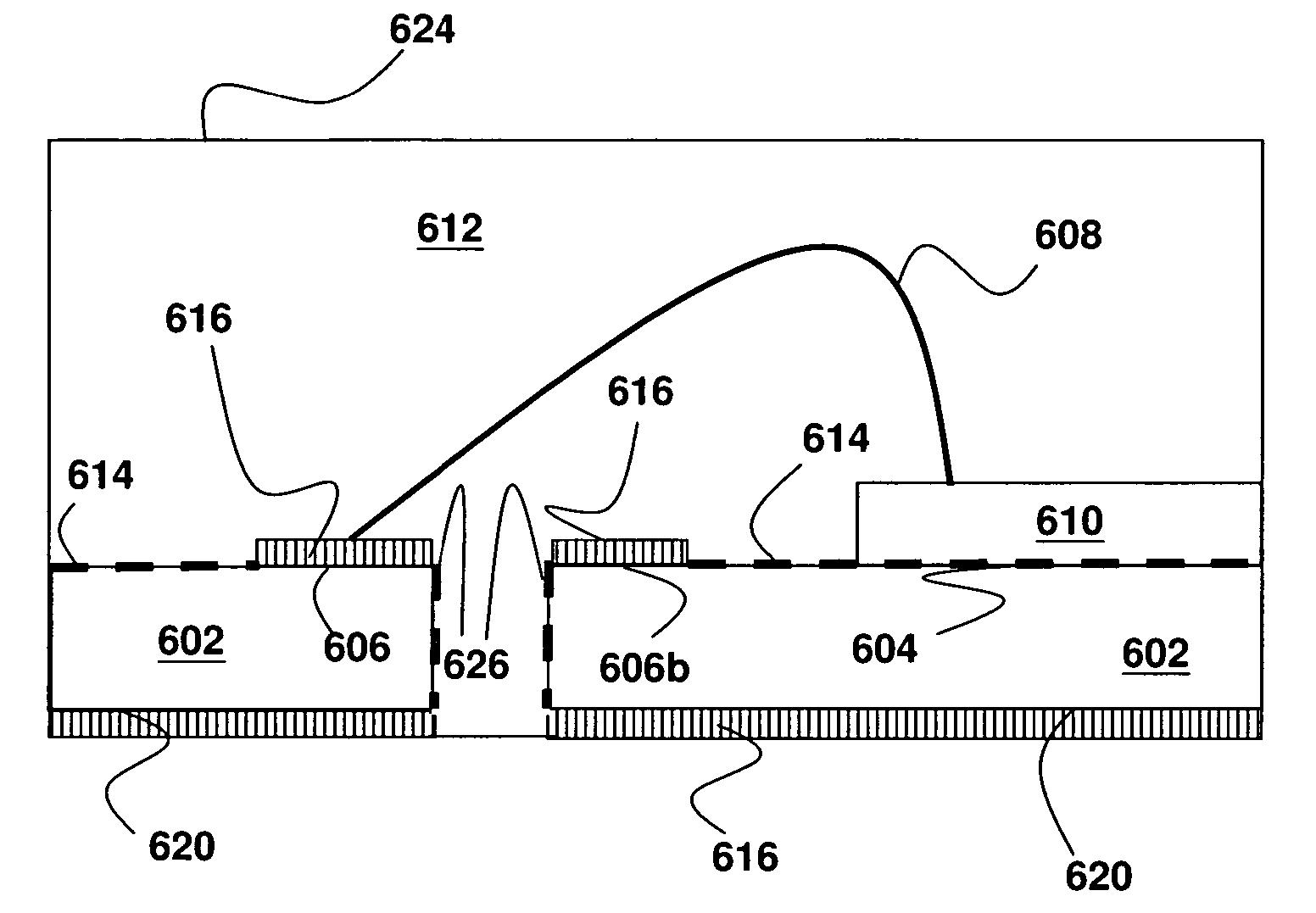
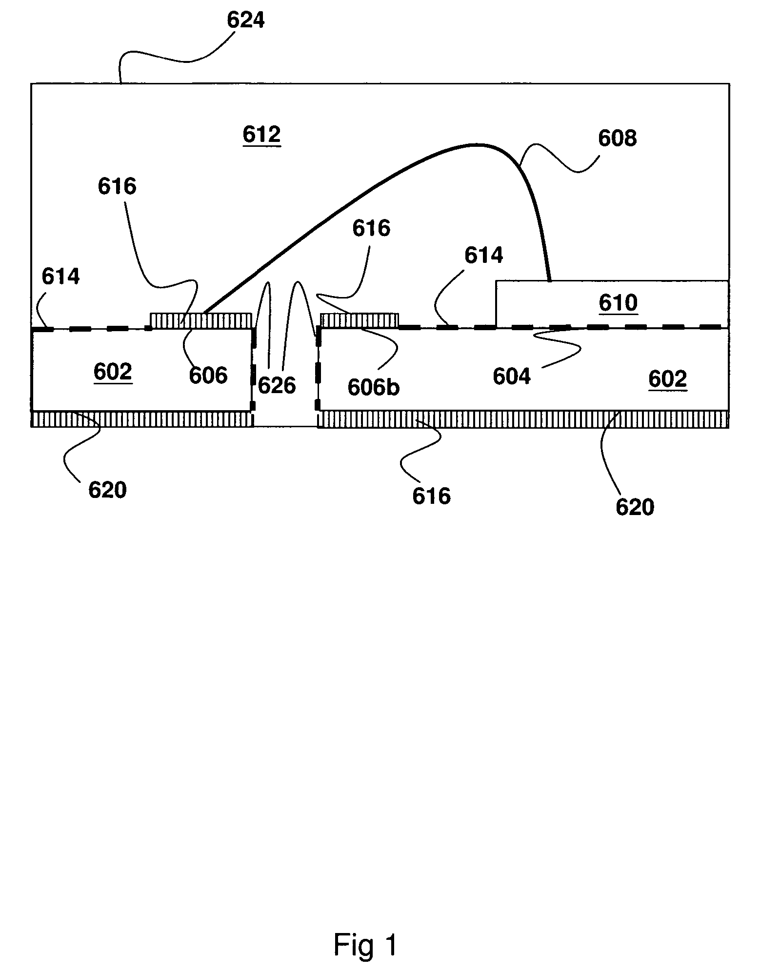
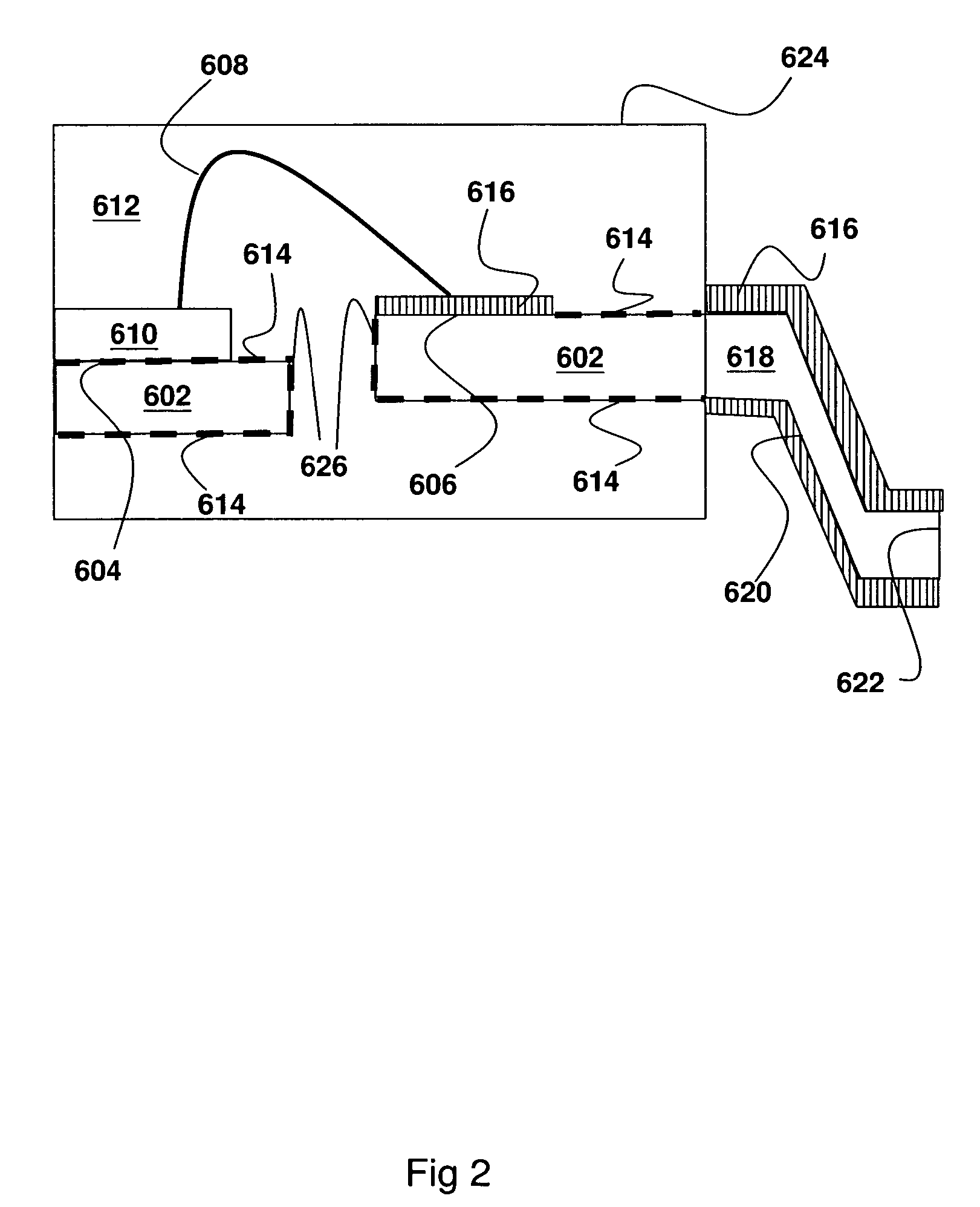
[0014]As used herein and in the claims, an “electronic device” refers to an apparatus that carries out its functions electronically and contains the package or leadframe according to the present invention. The term “comprising” should be construed to mean “including but not limited to”. A “leadframe” refers to a metal frame that connects a packaged chip to an external circuit and provides a supporting platform with direct and / or indirect electrical interconnections for a die. “Selective plating” refers to a plating process wherein some predetermined surfaces on the leadframe are chosen to be plated.

[0015]Referring now to FIG. 1, the first embodiment of the present invention is an electronic device containing a leadframe 602 whereon a die 610 is attached to and wire bonded. The leadframe 602 further contains a bonding surface 606 for wire bonding of wire 608 with the die 610; a die attachment surface 604 on which the die 610 attaches; soldering surfaces 620 exposed to the exterior of...


PUM

PropertyMeasurementUnit
temperatureaaaaaaaaaa
adhesionaaaaaaaaaa
surface areaaaaaaaaaaa

Abstract

An electronic device comprises a leadframe attached to a die and embedded in a mold packaging with enhanced adhesion property. The leadframe comprises a bonding surface, a soldering surface, a mold adhesion surface, and a die attachment surface wherein the soldering surface and bonding surface are selectively plated with nickel / palladium / gold. The mold adhesion surface and the die attachment surface are roughened for better attachment to a mold and a die respectively.

Description

FIELD OF INVENTION[0001]This invention relates to electronic devices with enhanced adhesion property, and in particular die packages and leadframes used therefor. This invention also relates to methods of making such electronic devices and leadframes.BACKGROUND OF INVENTION[0002]With the increasingly stringent requirement worldwide for environmentally friendly products, electronic devices that include heavy metals such as lead are likely to be slowly phased out. Therefore, electronic devices using bare copper as the soldering surfaces are slowly being replaced by those plated with other materials on such surfaces. Full plating of nickel / palladium / gold (Ni / Pd / Au) on all surfaces of the leadframe can avoid employing lead on the soldering surfaces; however, such surfaces have reduced adhesion to the molding compound.[0003]It is therefore an object of the present invention to provide an improved leadframe.SUMMARY OF INVENTION[0004]Accordingly, the present invention provides in one aspec...

Claims


Application Information

Patent Timeline
Patent Type & Authority Patents(United States)
IPC IPC(8): H01L23/495
CPCH01L23/3107H01L23/49582H01L24/48H01L2224/05155H01L2224/05644H01L2224/05664H01L2224/48091H01L2224/48247H01L2224/484H01L2224/85444H01L2224/85455H01L2224/85464H01L2924/01005H01L2924/01028H01L2924/01029H01L2924/01046H01L2924/01078H01L2924/01079H01L2924/01082H01L2924/014H01L2924/00014H01L2924/01006H01L2924/01033H01L2224/45099H01L2924/181H01L2924/00012
Inventor MARTIN, JOSEPH ANDREWFU, KING YIN FREDPHEN, HOI PING PATRICK
Owner QPL LTD
Why Eureka
Try Eureka