Single-event-effect tolerant SOI-based inverter, NAND element, NOR element, semiconductor memory device and data latch circuit

a soi-based inverter and memory device technology, applied in logic circuits, pulse techniques, reliability increasing modifications, etc., can solve problems such as serious malfunction or inversion of stored information, inability to realistically approach, and malfunction of elements, so as to and effectively prevent the occurrence of malfunction

Inactive Publication Date: 2009-03-17
JAPAN AEROSPACE EXPLORATION AGENCY
View PDF10 Cites 27 Cited by
  • Summary
  • Abstract
  • Description
  • Claims
  • Application Information

AI Technical Summary

Benefits of technology

[0032]As above, in the present invention, each of the p-channel MOS transistors and the n-channel MOS transistor of the inverter is connected in series with an additional MOS transistor having a channel of the same conductive type as that thereof, to formed a double structure, and respective nodes between the two p-channel MOS transistors and between the two n-channel MOS transistors are connected together through a connection line. Thus, the single event transient (SET) becomes less likely to occur, because a potential difference between the source and drain in each of the two MOS transistors between two lines connected to the connection line becomes approximately zero. Even if one of the remaining MOS transistors is turned on from its OFF state due to the SET, an inverter output becomes less affected thereby. This makes it possible to obtain an effect of being able to provide an SEE tolerant inverter capable of effectively preventing the occurrence of a malfunction due to SEE.
[0033]In the present invention, a memory element includes a storage node comprising two of the SEE tolerant inverters having respective outputs cross-connected to respective inputs thereof. This makes it possible to obtain an effect of being able to provide an SEE tolerant memory element capable of effectively preventing the occurrence of a malfunction due to SEE.
[0034]In the present invention, a data latch circuit includes a storage node comprising two of the SEE tolerant inverters, and one additional MOS transistor is connected in series with each of a p-channel MOS transistor and a n-channel MOS transistor included in a clocked inverter in a data input stage and connected to a clock. This makes it possible to obtain an effect of being able to provide an SEE tolerant data latch circuit capable of effectively preventing the occurrence of a malfunction due to SEE.
[0035]In the present invention, each of two or three p-channel MOS transistors and two or three n-channel MOS transistors in either one of a 2-input NAND element, 3-input NAND element, 2-input NOR element and 3-input NOR element, is combined with an additional MOS transistor having a channel of the same conductive type as that thereof and a gate interconnected to a gate thereof, in such a manner that their channels are connected in series, so as to form a double structure. This makes it possible to obtain an effect of being able to provide a 2-input NAND element, a 3-input NAND element, 2-input NOR element and 3-input NOR element each capable of effectively preventing the occurrence of a malfunction due to SEE.

Problems solved by technology

The generated electric charges may cause the so-called “single-event transient phenomenon” that they flow in various regions of the inverter according to electric fields in the elements, and the occurrence of such phenomenon leads to malfunctions of the elements, for example, transiently flipping or inverting an output of the inverter.
The phenomenon occurring in an inverter constituting a memory device is likely to cause a serious malfunction or inversion of stored information.
While it is contemplated to fully shield the high-energy particles in a physical or mechanical manner so as to prevent SEE, such an approach is not realistic.
As above, the conventional inverter and the conventional memory device including such an inverter are extremely susceptible to SEE.

Method used


Image

  • Single-event-effect tolerant SOI-based inverter, NAND element, NOR element, semiconductor memory device and data latch circuit
  • Single-event-effect tolerant SOI-based inverter, NAND element, NOR element, semiconductor memory device and data latch circuit
  • Single-event-effect tolerant SOI-based inverter, NAND element, NOR element, semiconductor memory device and data latch circuit

Examples


first embodiment

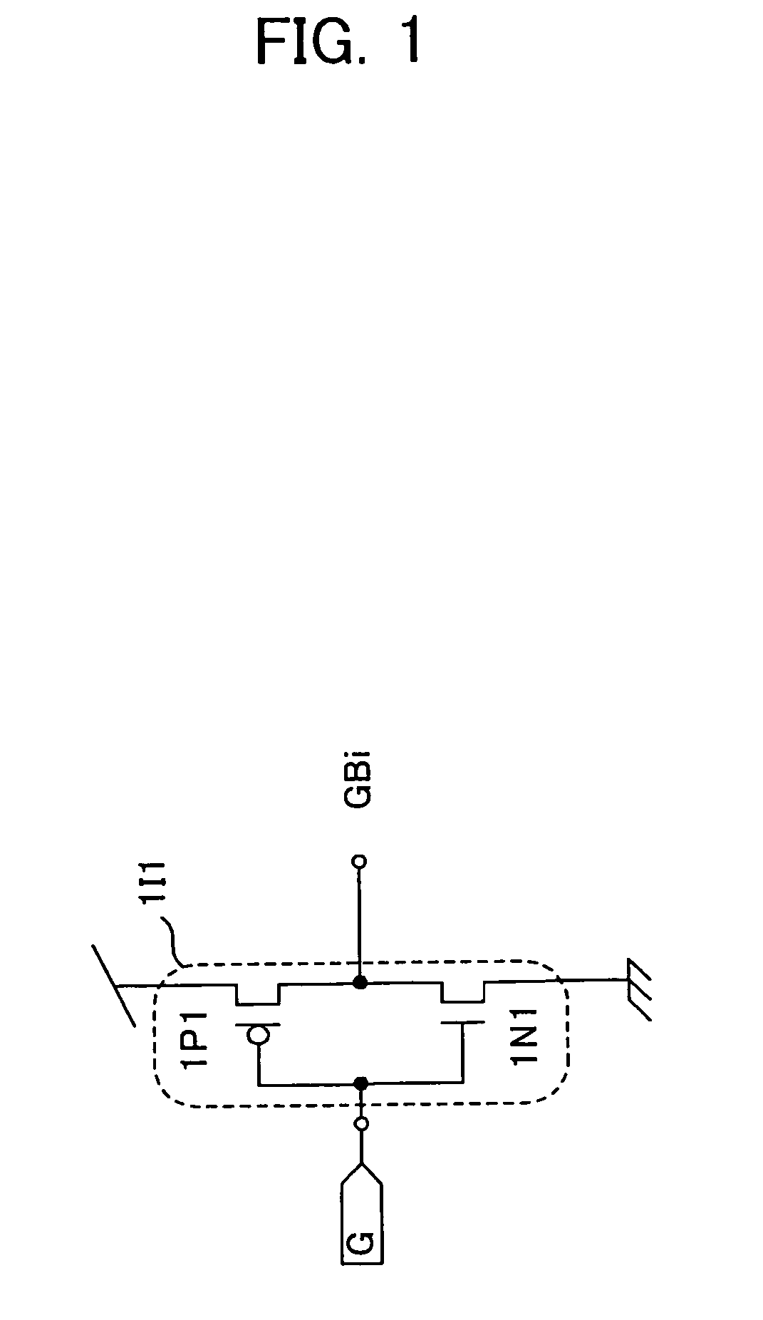
[0052](Configuration of Inverter of the Present Invention)

[0053]With reference to the circuit diagrams (FIGS. 4 to 6), respective configurations and operations of an inverter and a data latch circuit according to one embodiment of the present invention will now be described. FIG. 4 is a diagram showing the configuration of an inverter 3I including a double-structured transistor, according to a first embodiment of the present invention. In the inverter 3I, a (p-channel MOS) transistor 3P1 corresponding to the transistor 1P1 in the inverter 1I1 is combined with a (p-channel MOS) transistor 3P2 having a channel of the same conductive type as that thereof (p-channel MOS) and a gate connected to a gate thereof, in such a manner that they are connected in series with respect to a source or drain line, so as to form a double structure. The two transistors 3P1, 3P2 have a common gate, and their source or drain line to be controlled by the gate are connected in series with each other. Thus,...

second embodiment

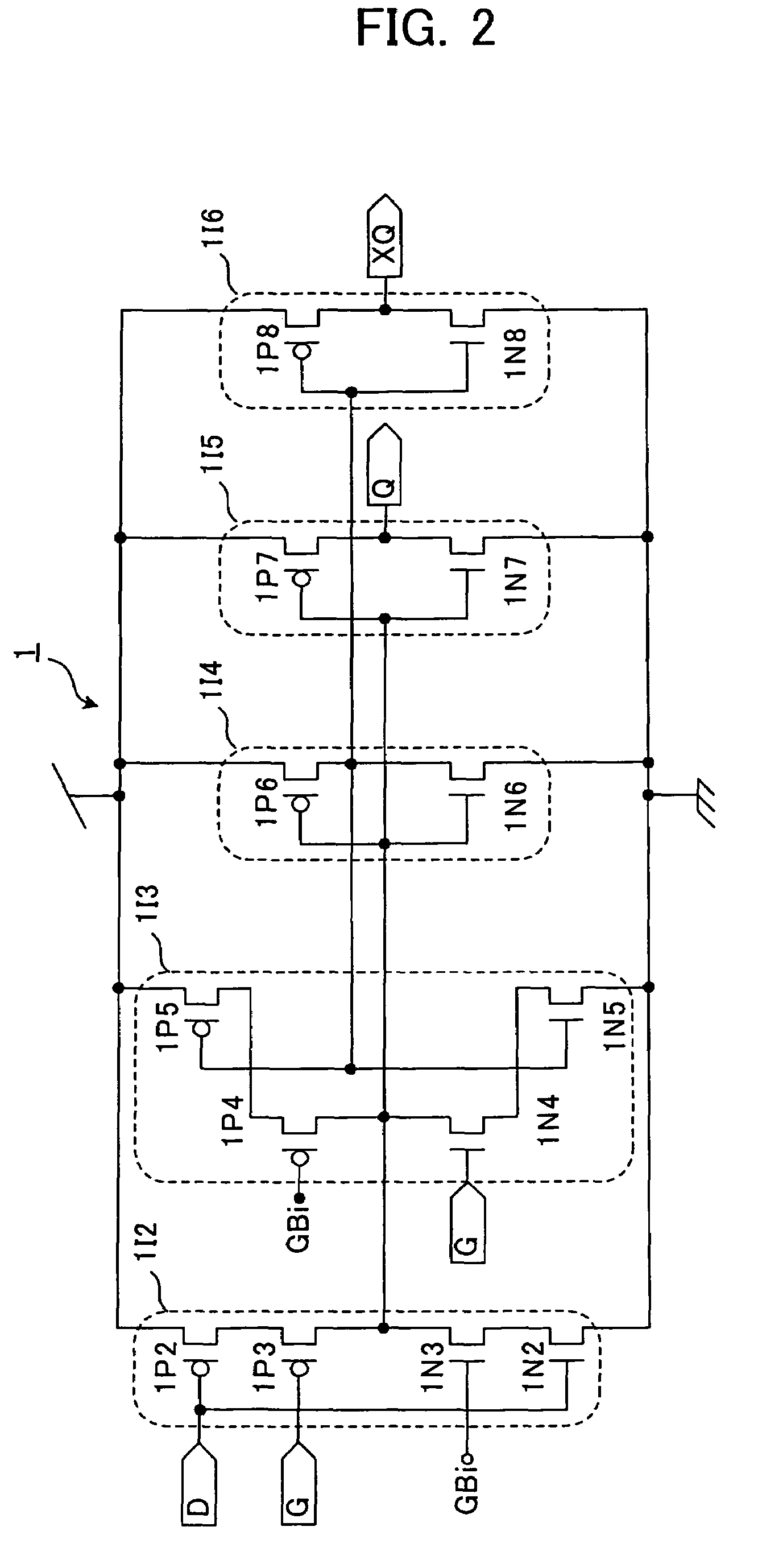
[0061](Memory Element of the Present Invention)

[0062]A memory element according to a second embodiment of the present invention will be described. A storage node can be obtained by cross-connecting respective outputs and inputs of two inverters directly or indirectly through a switching gate. For example, a memory element with such a storage node includes a SRAM (Static RAM), a flip-flop circuit and a latch circuit. Although not shown, the memory element according to the second embodiment has a storage node comprising at least two inverters each having the same configuration as that of the inverter 3I according to the first embodiment. This makes it possible to achieve a memory element having enhanced SEE tolerance. In this memory element, each of the inverters forming the storage mode has the same operation as that of the inverter 3I according to the first embodiment.

third embodiment

[0063](Data Latch Circuit of the Present Invention)

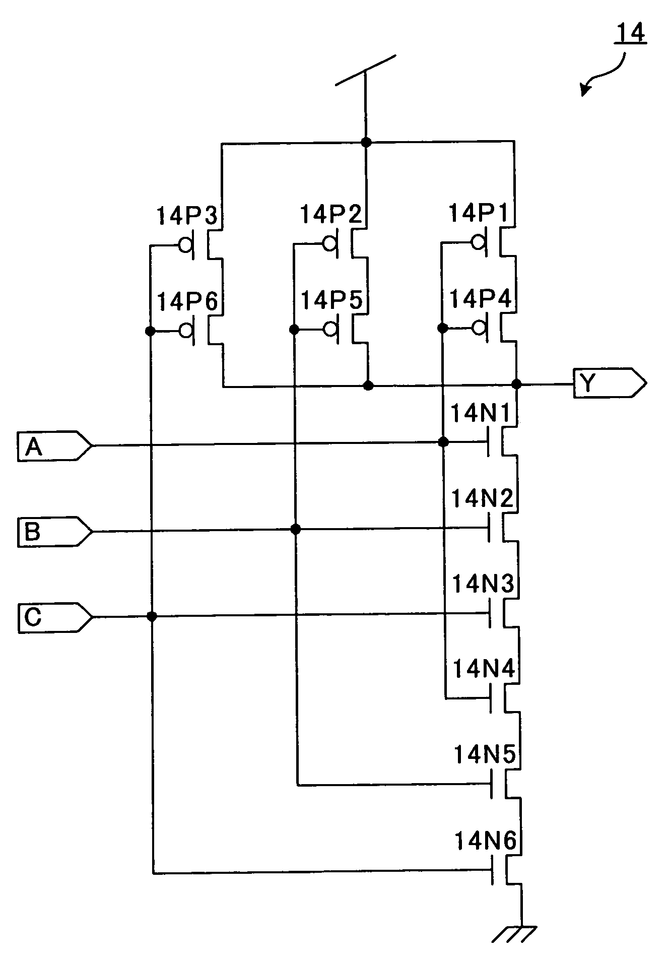
[0064]A data latch circuit 4 according to a third embodiment of the present invention will be described below. Firstly, the configuration of this data latch circuit 4 will be described. FIG. 6 is a circuit diagram of the data latch circuit 4. A buffer circuit 4B illustrated in FIG. 5 is used in combination with the data latch circuit 4 to shape a waveform of a clock signal G and an inverted clock signal GBi which are input into the data latch circuit 4. The buffer circuit 4B includes an inverter 4I1 and an inverter 4I2 which are connected to each other in a cascade arrangement. Viewed as a whole, the buffer circuit 4B generally comprises a clocked inverter 413 serving as an input stage, a transmission gate 4S1, the inverter 4I4 and the inverter 4I2.

[0065]The clocked inverter 4I1 comprises a p-channel MOS transistor 4P3, a p-channel MOS transistor 4P4, a p-channel MOS transistor 4P5, an n-channel MOS transistor 4N5, an n-channel MOS...


PUM


Abstract

Disclosed is an inverter, a NAND element, a NOR element, a memory element and a data latch circuit which exhibit high tolerance to single event effect (SEE). In an SEE tolerant inverter (3I), each of a p-channel MOS transistor and a n-channel MOS transistor which form an inverter is connected in series with an additional second transistor of the same conductive type as that thereof so as to form a double structure (3P1, 3P2; 3N1, 3N2). Further, a node A between the two p-channel MOS transistors and a node (B) between the two n-channel MOS transistors are connected together through a connection line. Each of an SEE tolerant memory element and an SEE tolerant data latch circuit comprises this SEE tolerant inverter (3I).

Description

CROSS-REFERENCE TO RELATED APPLICATIONS[0001]This is a continuation of prior International Patent Application No. PCT / JP2005 / 001675, filed on Feb. 4, 2005, which claims priority from Japanese Patent Application No. 2004-27818, filed on Feb. 4, 2004, each of which is incorporated herein by reference in its entirety.TECHNICAL FIELD[0002]The present invention relates to an SOI (Silicon-On-Insulator)-based inverter, an SOI-based memory device and an SOI-based data latch circuit, and more specifically to SEE (Single Event Effect)-tolerant SOI-based inverter, an SEE-tolerant SOI-based memory device and an SEE-tolerant SOI-based data latch circuit. The present invention further relates to an SOI-based NAND element and an SOI-based NOR element, and more specifically to an SEE-tolerant SOI-based NAND element and an SEE-tolerant SOI-based NOR element.BACKGROUND ART[0003]A semiconductor device, such as a memory device or a data latch circuit, has a storage node consisting of a combination of t...

Claims


Application Information

Patent Timeline
Patent Type & Authority Patents(United States)
IPC IPC(8): H03K19/003H03K19/094
CPCH03K19/00338
Inventor KUBOYAMA, SATOSHISHINDOU, HIROYUKIIIDE, YOSHIYAMAKIHARA, AKIKO
Owner JAPAN AEROSPACE EXPLORATION AGENCY
Why Eureka
Try Eureka