MEMS capacitive bending and axial strain sensor

a capacitive bending and axial strain sensor technology, applied in the field of strain sensors, can solve the problems of preventing a clear determination, affecting the quality of the sensor, and not having a sensor that can measure bending and axial strain, and achieves the effect of low power and easy incorporation into the current semi-conductor fabrication process

Active Publication Date: 2009-03-31
GLOBUS MEDICAL INC
View PDF21 Cites 27 Cited by
  • Summary
  • Abstract
  • Description
  • Claims
  • Application Information

AI Technical Summary

Benefits of technology

[0013]Advantages of this system allow the sensor to use very low power since the method of actuation is mechanical. This allows the system to be incorporated in implantable and wireless medical device systems that do not require the use of a battery. Fabrication of the device does not require expensive silicon-on-insulator wafers and the sensor can easily be incorporated into current semi-conductor fabrication processes.

Problems solved by technology

However, image obstructions often prevent a clear determination if fusion has occurred.
However, there has not been a sensor available that can measure bending and axial strain in a capacitive manner.
U.S. Pat. No. 5,827,980 to Doemens (1998) has developed a dual comb structure; however, the orientation of the device is situated at 45 degrees and is not meant to observe bending strain.
However, bending is not the primary method of actuation which would cause the comb structures to move vertically causing a change in the overlapping surface area.
However, due to the attachment method of securing both ends of the comb structures to the substrate, the sensor would not be able to actuate while undergoing bending strain.
A similar case is made with U.S. Pat. No. 7,035,083 to Lin (2006), where the attachment method of the tines will not allow vertical displacement allowing a change in the overlapping surface area of the tines.
However, the lack of vertical dimension or overlapping surface area can not be used to determine the amount of bending strain present in a deformed substrate.

Method used


Image

  • MEMS capacitive bending and axial strain sensor
  • MEMS capacitive bending and axial strain sensor
  • MEMS capacitive bending and axial strain sensor

Examples


Embodiment Construction

[0025]The present invention will now be described more fully with reference to the drawings, in which illustrative embodiments are shown.

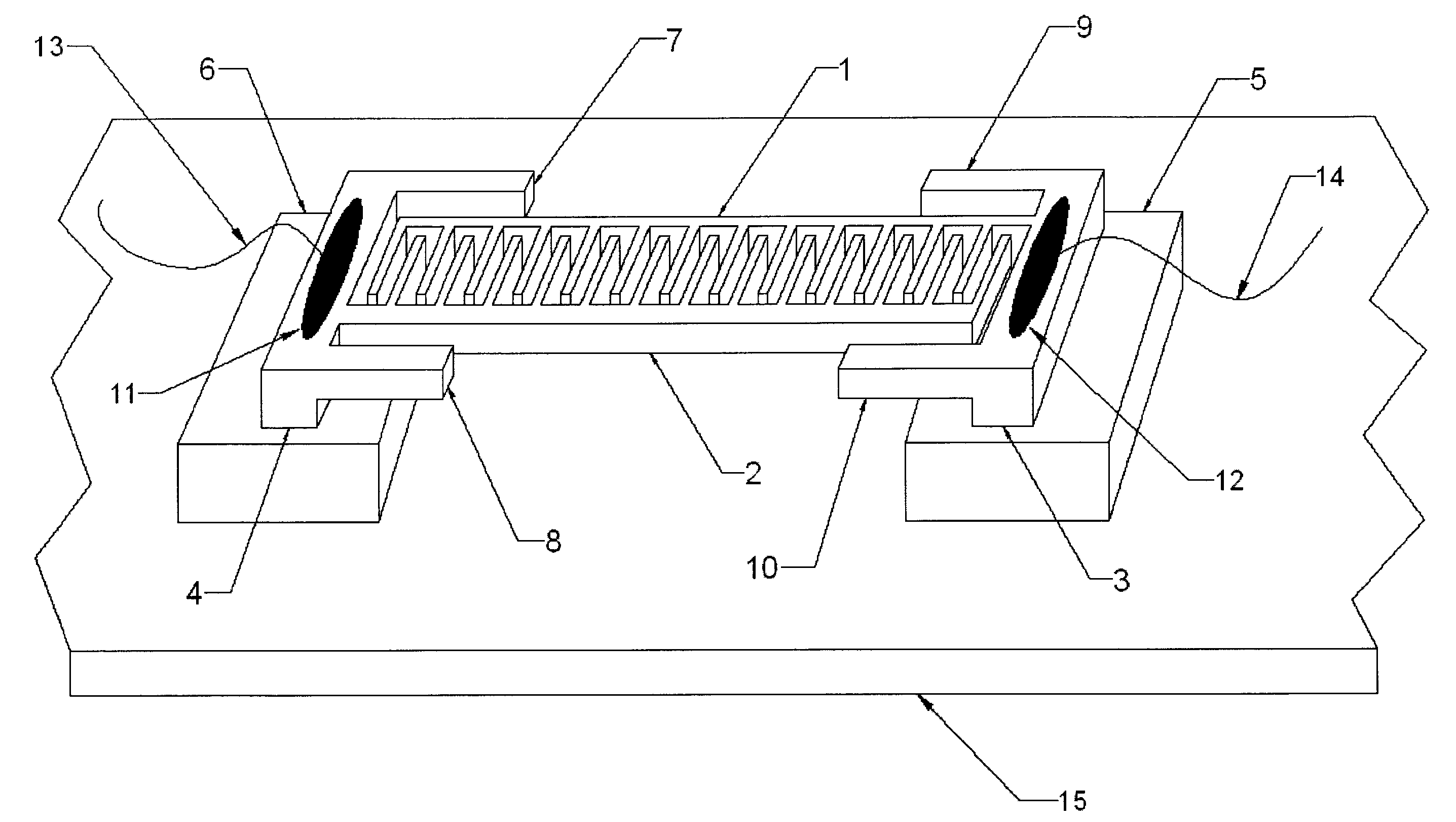
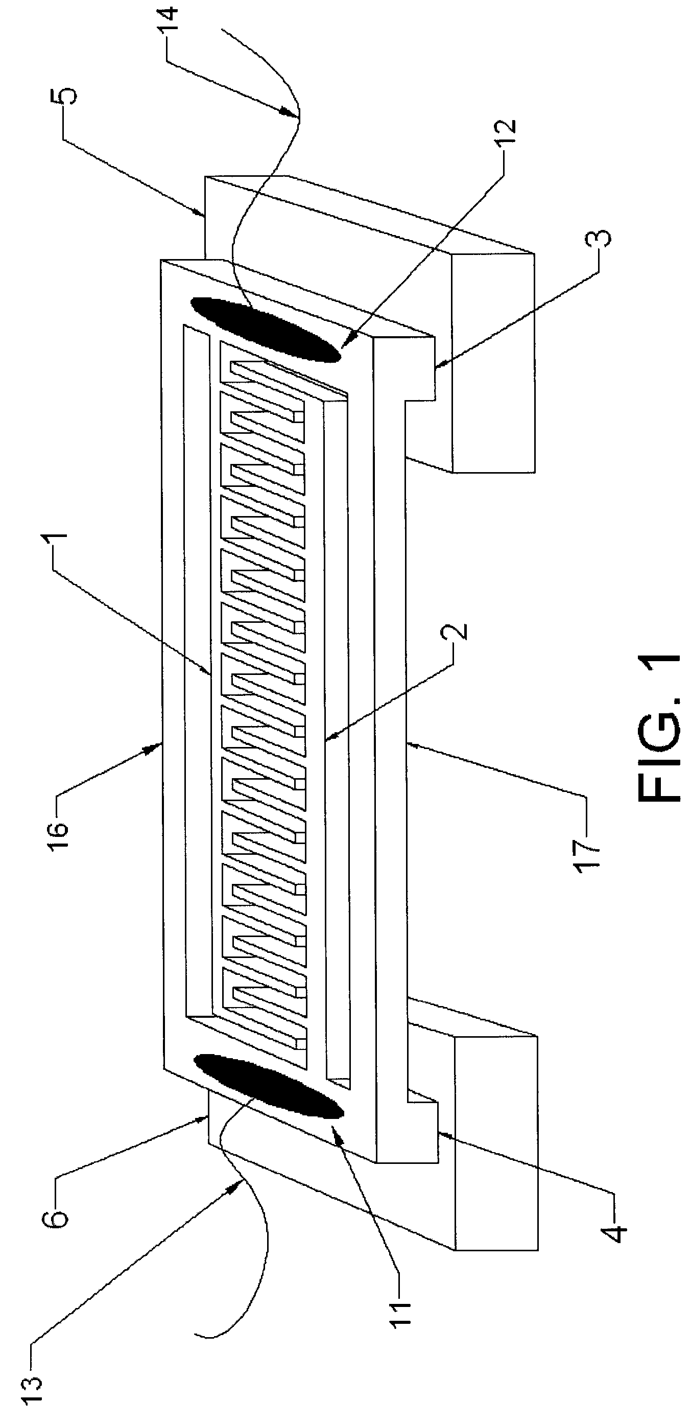
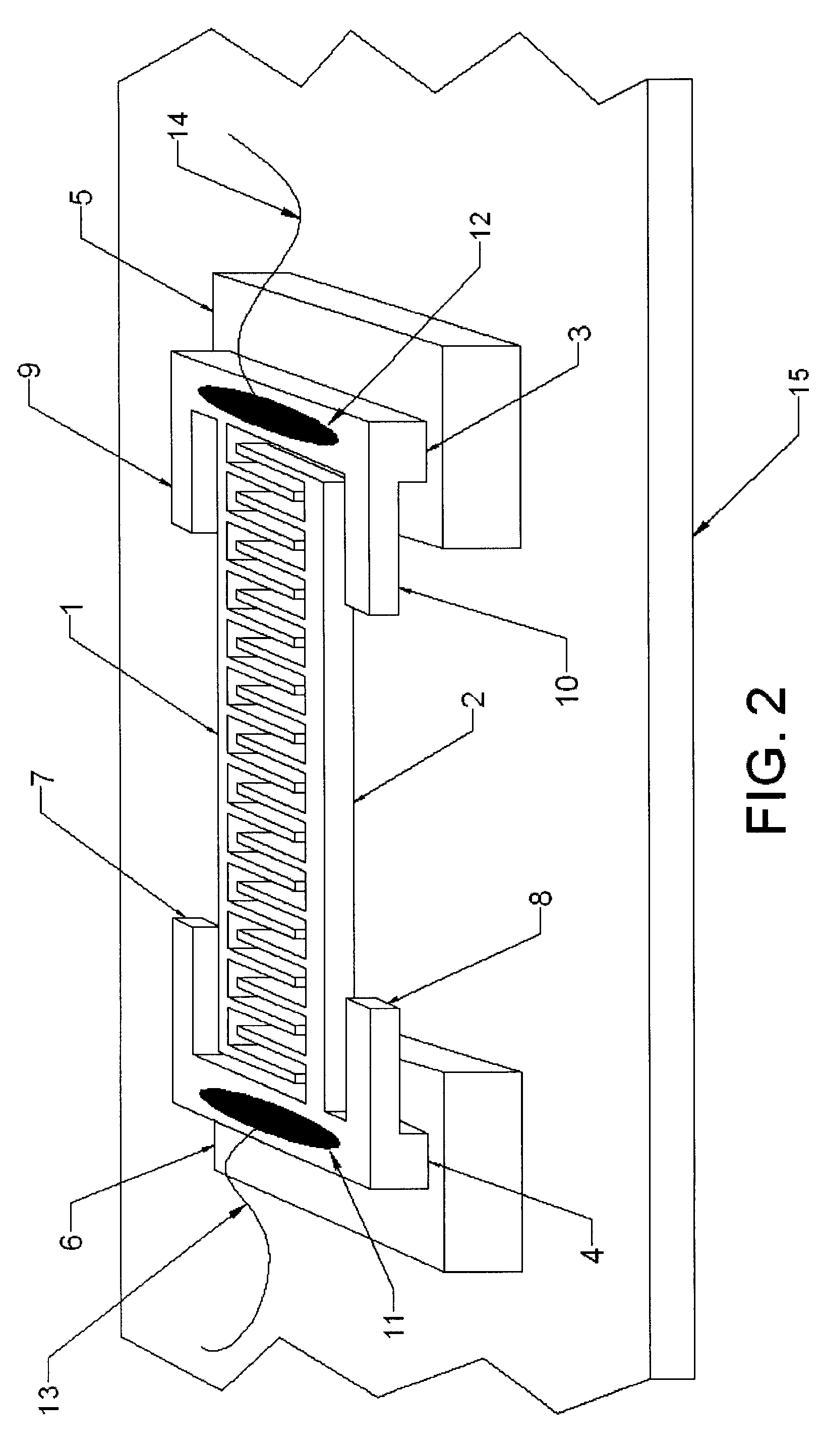
[0026]FIG. 1 is an perspective view of the three-dimensional micro-electromechanical-systems MEMS capacitive bending and axial strain sensor before it is affixed to a flat substrate in which the movable silicon comb structures 1, 2 containing the suspended interdigitated fingers are fabricated using conventional semiconductor fabrication techniques. Each comb structure 1, 2 is elevated by an anchor 3, 4 incorporated at the end the comb structure 1, 2. A glass pad 5, 6 is anodically bonded to the bottom of each anchor 3, 4 to provide electrical isolation from the substrate and to increase the distance from the substrate to the plane of the interdigitated fingers to improve sensitivity. Electrically conductive epoxy 11, 2 is applied to the top of each anchor 3, 4. Electrical leads or wires 13, 14 are placed in the electrically conductive epoxy 11, 12...


PUM

PropertyMeasurementUnit
relative permittivityaaaaaaaaaa
capacitanceaaaaaaaaaa
non-conductiveaaaaaaaaaa

Abstract

A three-dimensional micro-electro-mechanical-systems (MEMS) capacitive bending and axial strain sensor capacitor is described. Two independent comb structures, incorporating suspended polysilicon interdigitated fingers, are fabricated simultaneously on a substrate that can displace independently of each other while attached to a substrate undergoing bending or axial deformation. A change in spacing between the interdigitated fingers will output a change in capacitance of the sensor and is the primary mode of operation of the device. On the bottom and to the end of each comb structure, a glass pad is attached to the comb structure to allow for ample surface area for affixing the sensor to a substrate. During fabrication, tethers are used to connect each comb structure to maintain equal spacing between the fingers before attachment to the substrate. After attachment, the tethers are broken to allow independent movement of each comb structure.

Description

CROSS-REFERENCE TO RELATED APPLICATIONS[0001]This application claims the benefit of provisional patent Appl. No. 60 / 730,087, of the same title filed 2005 Oct. 26 by the present inventor, the disclosure of which is hereby incorporated by reference in its entirety.FEDERALLY SPONSORED RESEARCH[0002]This invention was made with government assistance provided by the National Science Foundation under Contract No. BES-0097521. The government has certain rights to this invention.BACKGROUND OF THE INVENTION-FIELD OF INVENTION[0003]This invention relates to a strain sensor, specifically to a sensor that can measure axial and bending strain.BACKGROUND OF THE INVENTION[0004]Variable capacitors play a fundamental role in high-frequency and radio-frequency (RF) circuits. In the last few years, MEMS variable capacitors have drawn considerable interest due to their superior electrical characteristics, size and cost of manufacture.[0005]While variable capacitors using MEMS technology can be readily ...

Claims


Application Information

Patent Timeline
Patent Type & Authority Patents(United States)
IPC IPC(8): G01L1/14
CPCG01L1/148
Inventor AEBERSOLD, JULIA W.WALSH, KEVINCRAIN, MARKVOOR, MICHAEL
Owner GLOBUS MEDICAL INC
Why Eureka
Try Eureka