Register configuration control device, register configuration control method, and program for implementing the method

a configuration control and register technology, applied in the field of register configuration control devices, register configuration control methods, program for implementing methods, can solve the problems of reducing the frame rate of an image, increasing the circuit scale of the display processing device, and cpu if the circuit b>202/b> cannot complete the writing of configuration data into the register

Inactive Publication Date: 2009-03-31
CANON KK
View PDF4 Cites 9 Cited by
  • Summary
  • Abstract
  • Description
  • Claims
  • Application Information

AI Technical Summary

Benefits of technology

[0015]It is an object of the present invention to provide a resister configuration control device, and a resister configuration control method, which make it possible to update resister configuration values during a non-display period without increasing a circuit scale, and a program for implementing the method.
[0018]As a consequence, it is no longer necessary to provide registers configured in two stages, and an increase in the circuit scale can be prevented. Further, it is possible to perform simultaneous configuration (updating) of registers at high speed in designated timing during a non-display period (blanking period).
[0019]Furthermore, by using adjacent areas in a memory space for temporary storage, it is possible to concentrate memory areas for use in register configuration, thereby reducing the memory space for use in temporary storage.

Problems solved by technology

However, if the non-display period is short, there is a fear that the CPU IF circuit 202 cannot complete writing of configuration data into the register groups 203 to 205.
However, this method causes reduction of a frame rate of an image.
This brings about the problem of an increased circuit scale of the display processing device.

Method used


Image

  • Register configuration control device, register configuration control method, and program for implementing the method
  • Register configuration control device, register configuration control method, and program for implementing the method
  • Register configuration control device, register configuration control method, and program for implementing the method

Examples


first embodiment

[0060]First, a description will be given of the present invention with reference to the drawing.

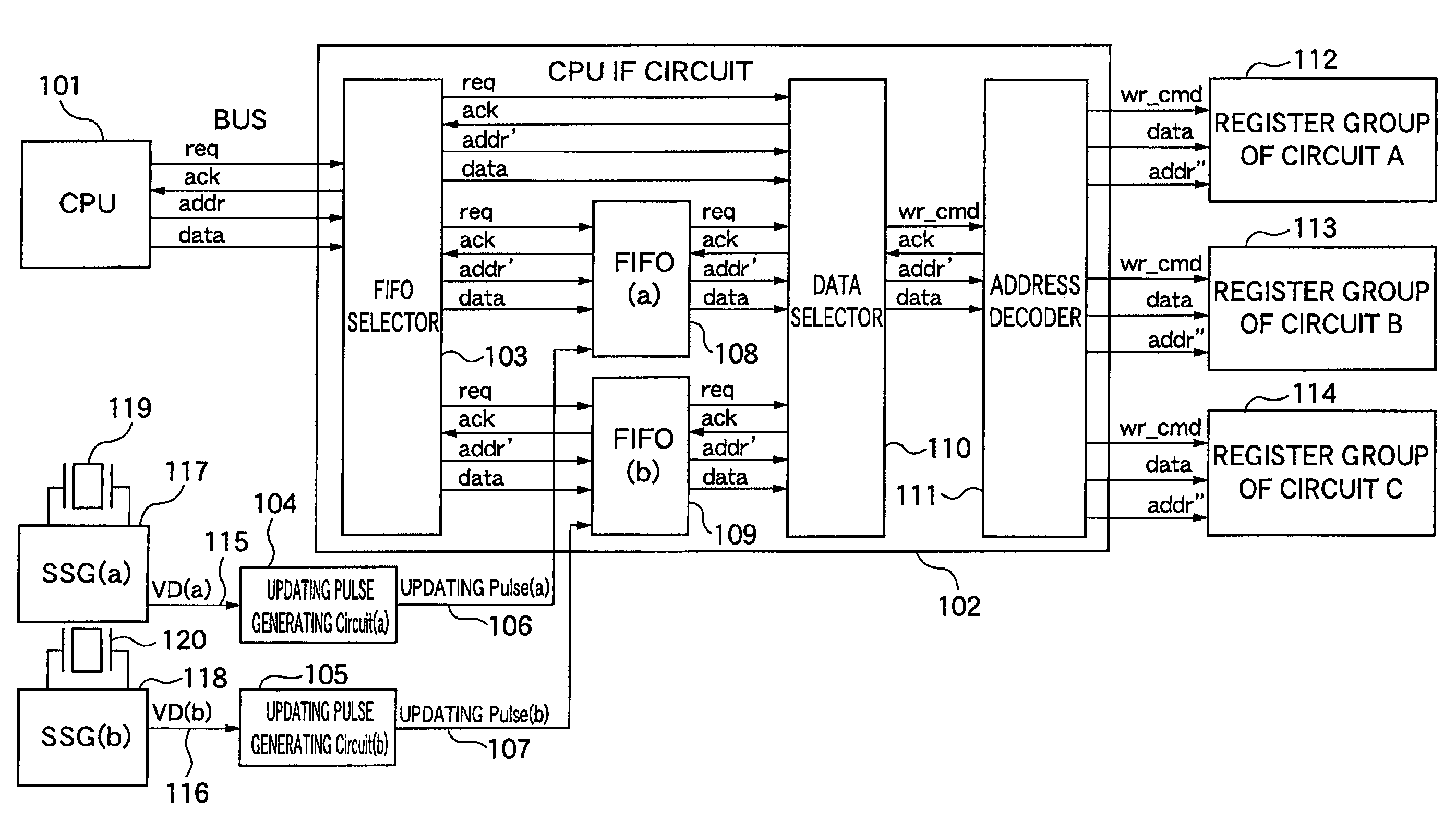
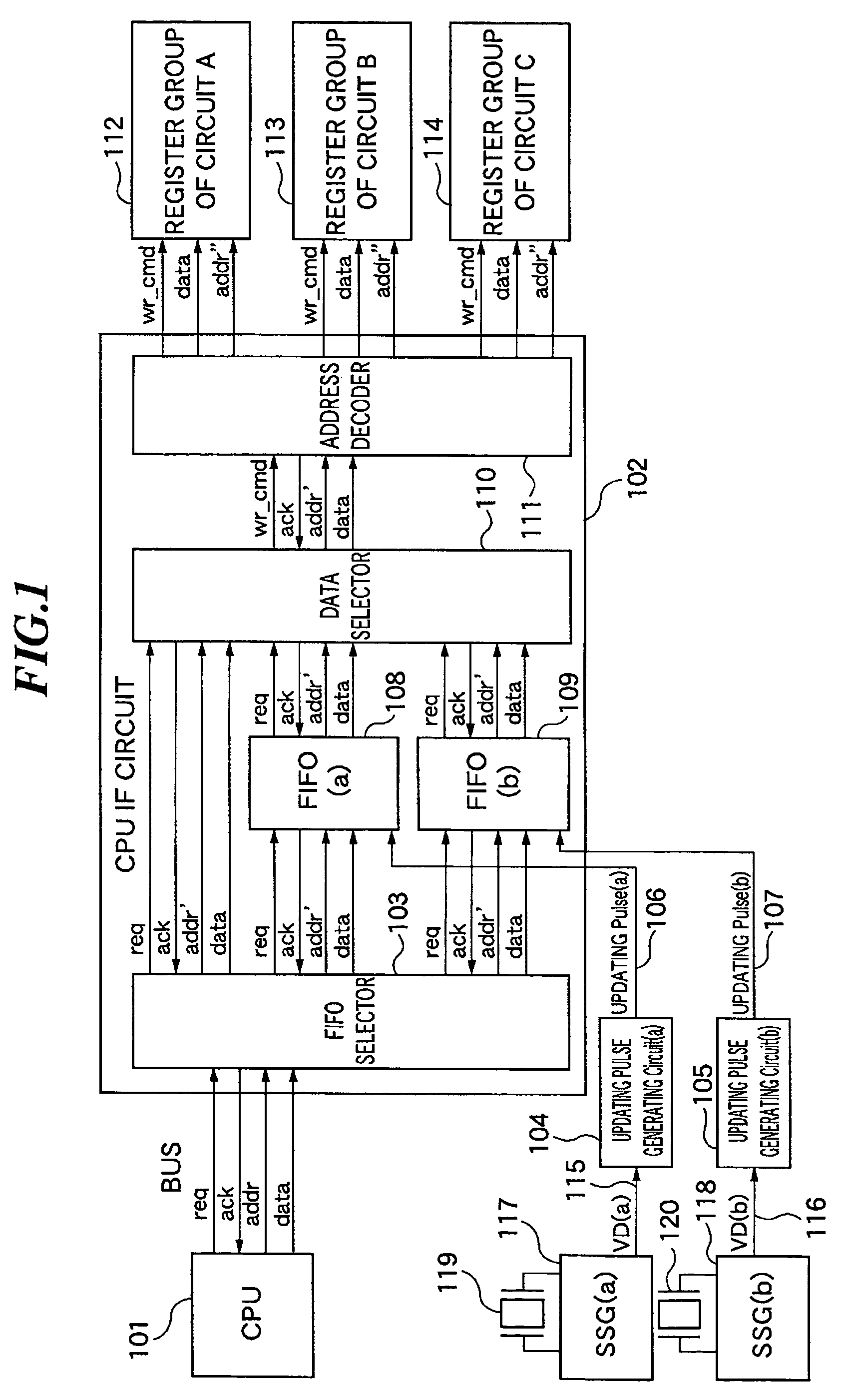
[0061]FIG. 1 is a block diagram of a register configuration control device according to the first embodiment. The register configuration control device performs register configurations for register groups including control registers for controlling an image pickup device and an image display device.

[0062]Referring to FIG. 1, a CPU 101 delivers a request signal (hereinafter referred to as “the signal req”), an acknowledge signal (hereinafter referred to as “the signal ack”), a 10-bit address signal (hereinafter referred to as “the signal addr”), and a 32-bit data signal (hereinafter referred to “the 32-bit signal data”) to a CPU interface (IF) circuit 102. These signals are for use in writing register configuration values in a register group 112 of a circuit A, a register group 113 of a circuit B, and a register group 114 of a circuit C, which are included in a control device for controlli...

second embodiment

[0108]Next, a description will be given of the present invention.

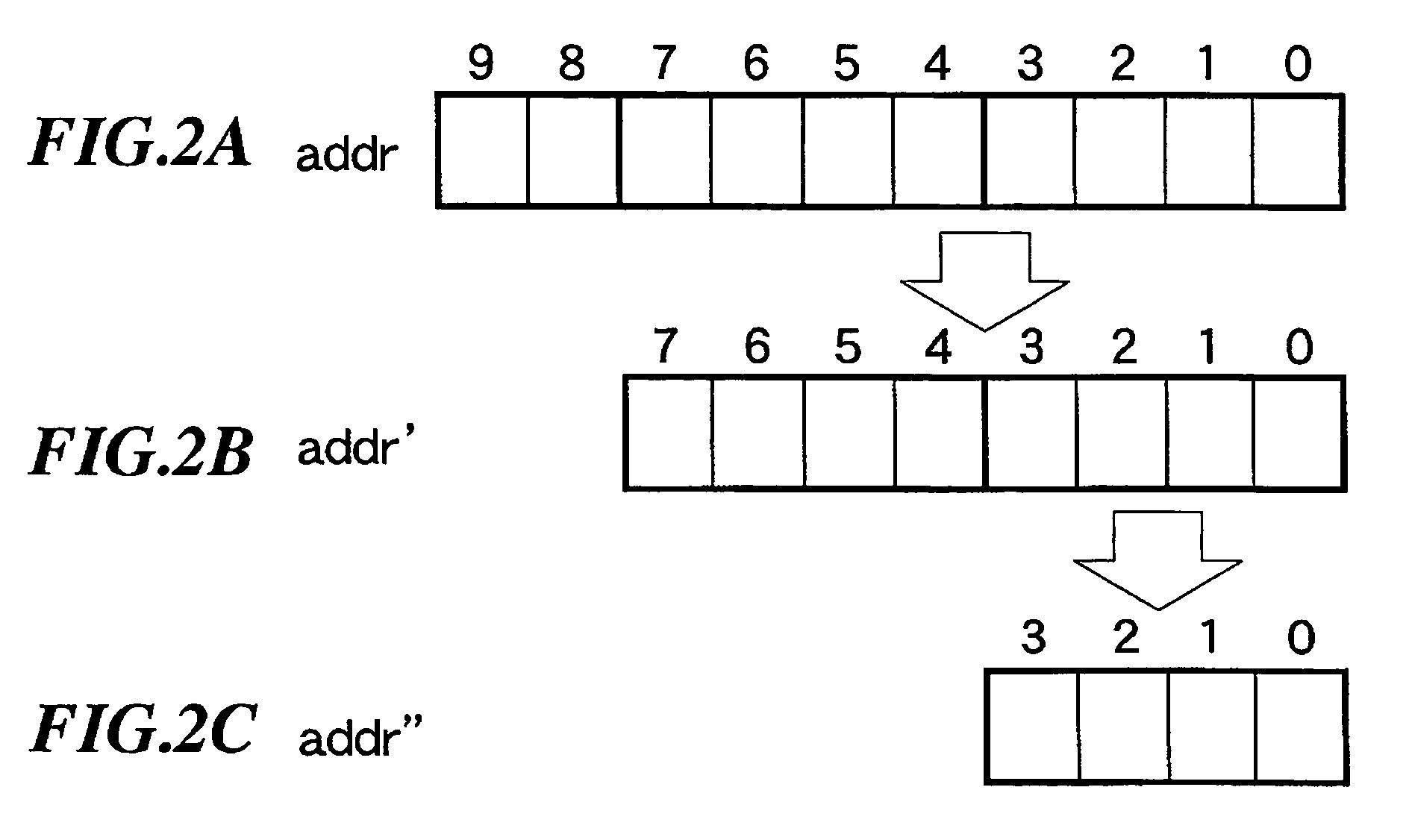
[0109]As shown in a memory map in FIG. 8, in the above described first embodiment, a memory associated with the bits 9-8 of the 10-bit address (addr) which are set to “11” is not used in a memory space formed by the whole of the register groups 112 to 114 of the circuits A to C. Further, memories which are assigned addresses indicated by the bits 7-0 set to respective values from “00110000” to “11111111” are not used in any of memory spaces associated with respective bits 9-8 of the address (addr) set to “00”, “01”, and “10”.

[0110]Therefore, in the second embodiment, an address assigned to each memory space is formed of 8 bits, as shown in a memory map illustrated in FIG. 9. Register configuration is performed directly from a CPU when the bits 7-4 are set to “0000”, “0001”, or “0010”, from a FIFO (a) when the bits 7-4 are set to “0011”, and from a FIFO (b) when the bits 7-4 are set to “0101”.

[0111]FIG. 10 is a block di...

third embodiment

[0159]Next, the present invention will be described.

[0160]In the following, a description will be given of how register configuration values having written in the FIFO 108 within the CPU IF circuit 102 during a video image pickup period are simultaneously set in some blocks in the image pickup apparatus, such as a digital camera, at high speed during the vertical blanking period.

[0161]FIG. 18 is a block diagram of the image pickup apparatus according to the third embodiment.

[0162]In FIG. 18, reference numeral 401 designates a lens, 402 a diaphragm, 403 an image pickup element that performs photoelectrical conversion, 404 an amplifier that performs amplification, noise removal, etc. on electric signals output from the image pickup element 403, 405 an A / D converter circuit that coverts an analog signal output from the amplifier 404 into a digital signal, 406 a color interpolation circuit that interpolates the digital signal from an RGB Bayer array into pixel-by-pixel (R, G, B) signals...


PUM


Abstract

A resister configuration control device which is capable of updating resister configuration values during a non-display period without increasing a circuit scale. A FIFO selector 103 receives register configuration value information comprising a register configuration value and address information, and selects a transmission destination to which the register configuration value information is to be sent, from FIFOs 108 and 109 based on the address information and sends the register configuration value information to the selected destination. The FIFO 108 or 109 temporarily stores the register configuration value information sent from the FIFO selector 103, and reads-out and outputs the register configuration value information in predetermined timing. A data selector 110 selects one of the register configuration value information sent from the FIFO selector 103 and the register configuration value information output from the FIFO 108 or 109, according to a predetermined priority, and outputs the selected register configuration value information.

Description

BACKGROUND OF THE INVENTION[0001]1. Field of the Invention[0002]The present invention relates to a register configuration control device for performing register configuration for peripheral circuits from a host CPU, a register configuration control method applied to the register configuration control device, and a program for causing a computer to execute the register configuration control method.[0003]2. Description of the Related Art[0004]Conventionally, there has been proposed a display processing device whose display output section for digitally processing video signals for display is controlled by a host CPU.[0005]FIG. 16 is a block diagram of the conventional display processing device.[0006]Referring to FIG. 16, the display output section is comprised of a CPU interface (CPU IF) circuit 202 and a plurality of register groups 203 to 205, and a host CPU 201 is connected to the display output section. The register groups 203 to 205 are storage devices for storing various kinds of...

Claims


Application Information

Patent Timeline
Patent Type & Authority Patents(United States)
IPC IPC(8): G11C7/00
CPCG06F3/14G06F9/4411G09G5/02G09G5/06G09G5/393G09G5/395G09G2310/061G09G2320/0285
Inventor HOUDA, SAORIRENGAKUJI, HIDEYUKI
Owner CANON KK
Why Eureka
Try Eureka