Grounding front-end-of-line structures on a SOI substrate

a front-end of line and substrate technology, applied in the direction of semiconductor devices, semiconductor/solid-state device details, electrical equipment, etc., can solve the problems of inability to test vc structures that require grounding of an active region, the above-described grounding technique does not work, and the ground path is not helpful for vc inspection of active region and gate stack structures

Active Publication Date: 2009-04-14
TAIWAN SEMICON MFG CO LTD
View PDF12 Cites 97 Cited by
  • Summary
  • Abstract
  • Description
  • Claims
  • Application Information

AI Technical Summary

Problems solved by technology

A number of challenges exist relative to building VC test structures.
One challenge is grounding front-end-of-line (FEOL) structures targeting the active region or gate stack levels, especially for silicon-on-insulator (SOI) technology.
However, with SOI technology, the buried oxide (BOX) layer presents an additional barrier so the above-described grounding technique does not work.
Design rules typically do not allow this level and the active region or gate stack levels to be coincident.
Unfortunately this ground path is not helpful for VC inspection for active region and gate stack structures because the ground path to the VC test structure is required when the test structure is still exposed at the wafer surface and visible to the SEM.
Therefore, VC test structures that require grounding of an active region are currently impossible for SOI technology.
First, special short loop wafers are necessary, which creates an additional cost.
Second, because the transistors will not work, very little other data can be collected for comparison.
Third, the process sequence is not entirely representative of the real process.
This technique also suffers from a number of drawbacks.
Secondly, a large plate of gate stack is often a design rule violation.
Again, this method is not useful for VC inspection because the ground path to the VC test structures is required when the test structures are still exposed at the wafer surface.

Method used


Image

  • Grounding front-end-of-line structures on a SOI substrate
  • Grounding front-end-of-line structures on a SOI substrate
  • Grounding front-end-of-line structures on a SOI substrate

Examples


Embodiment Construction

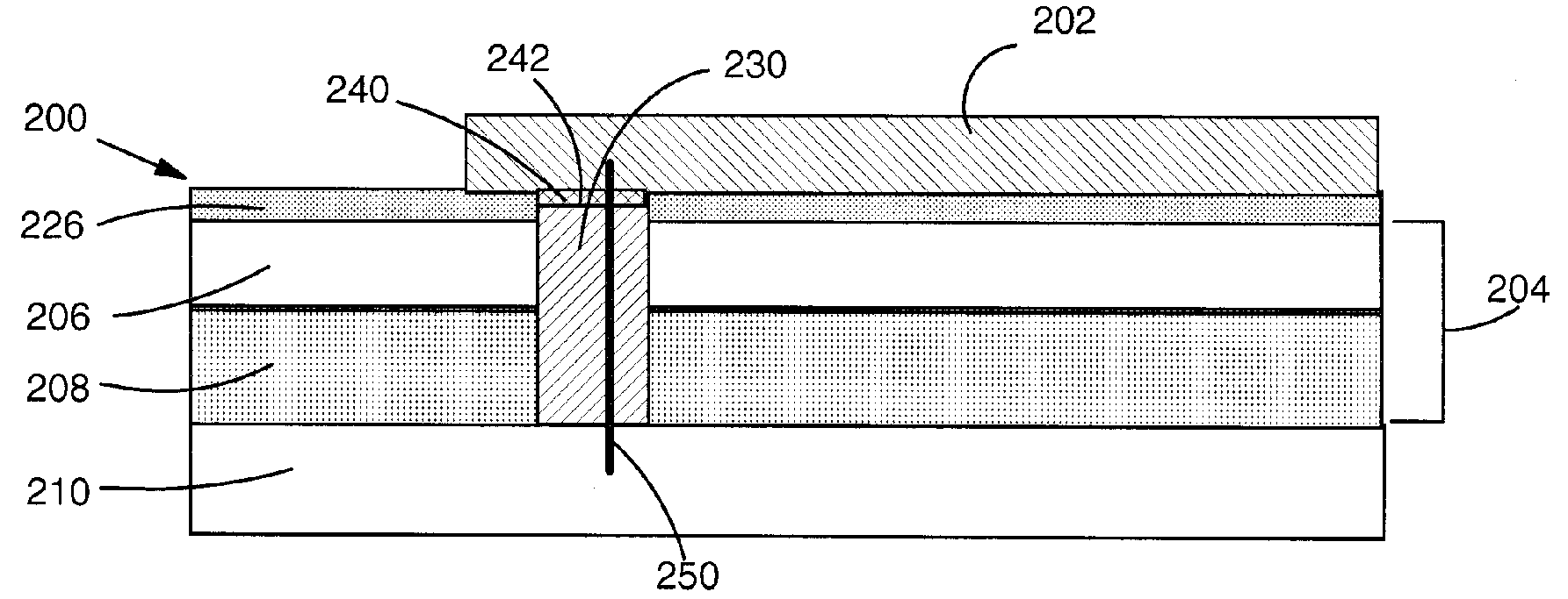
[0022]Turning to the drawings, FIG. 3 shows one embodiment of a structure 100 for grounding a silicon active region 102 within a silicon-on-insulator (SOI) substrate 104. SOI substrate 104 includes a silicon-on-insulator (SOI) layer 106 and a buried oxide (BOX) layer 108. Silicon active region 102 is provided within SOI layer 106. Structure 100 includes a bulk silicon substrate 110 having SOI substrate 104 thereover. As shown in the top view of FIG. 4, silicon active region 102 includes at least one finger element 120 within SOI layer 106 (FIG. 3). In one embodiment, a plurality of finger elements 120 are within SOI layer 106. Each finger element 120 is isolated by a shallow trench isolation (STI) region 122 of, for example, silicon dioxide (SiO2). For example, each finger element 120 is separated from an adjacent finger element 120 by STI region 122. STI region 122 is not shown in FIG. 3 because it has been replaced by polysilicon ground 130, as will be described below. FIG. 3 is v...


PUM


Abstract

Structures and a method are disclosed for grounding gate-stack and / or silicon active region front-end-of-line structures on a silicon-on-insulator (SOI) substrate, which may be used as test structures for VC inspection. In one embodiment, a structure includes a grounded bulk silicon substrate having the SOI substrate thereover, the SOI substrate including a silicon-on-insulator (SOI) layer and a buried oxide (BOX) layer; the silicon active region having at least one finger element within the SOI layer, the at least one finger element isolated by a shallow trench isolation (STI) layer; and a polysilicon ground intersecting the at least one finger element and extending through the STI layer and the BOX layer to the grounded bulk silicon substrate, the polysilicon ground contacting the silicon active region and the grounded bulk silicon substrate.

Description

BACKGROUND OF THE INVENTION[0001]1. Technical Field[0002]The invention relates generally to semiconductor fabrication, and more particularly, to structures and a method for grounding front-end-of-line (FEOL) structures, such as a gate stack or active region, through a silicon-on-insulator (SOI) substrate.[0003]2. Background Art[0004]In-line voltage contrast (VC) inspection is a powerful technique for detecting and isolating yield limiting defects in the semiconductor fabricating industry. In-line VC inspection includes scanning the wafer surface in which test structures exist with a scanning electron microscope (SEM). As the inspection proceeds, the SEM induces a charge on all electrically floating elements whereas any grounded elements remain at a zero potential. This potential difference is visible to the SEM. In particular, for electron landing energies less than the second crossover of the secondary electron yield curve (approximately 1.5 keV for tungsten (W) and copper (Cu)), g...

Claims


Application Information

Patent Timeline
Patent Type & Authority Patents(United States)
IPC IPC(8): H01L23/62
CPCH01L21/76264H01L21/84H01L27/1203
Inventor COTE, WILLIAM J.PATTERSON, OLIVER D.
Owner TAIWAN SEMICON MFG CO LTD
Why Eureka
Try Eureka