Power-MOSFETs with Improved Efficiency for Multi-channel Class-D Audio Amplifiers and Packaging Thereof

a technology of audio amplifiers and power mosfets, applied in the direction of amplifier combinations, low frequency amplifiers, and semiconductor/solid-state device details, can solve the problems of poor efficiency, high fidelity audio amplification using linear amplification, and excessive heating, and achieve low specific on-resistance and simple fabrication techniques.

Inactive Publication Date: 2008-10-16
ADVANCED ANALOGIC TECHNOLOGIES INCORPORATED
View PDF6 Cites 105 Cited by
  • Summary
  • Abstract
  • Description
  • Claims
  • Application Information

AI Technical Summary

Benefits of technology

[0035]The present invention includes several class D audio amplifiers that use vertical power MOSFET technology with low specific on-resistance and simple fabrication techniques. One such class D audio amplifier uses four P-channel high-side devices paired with four N-channel low-side devices as four half bridges. The N-channel devices share a common ground-connected source and have separate drain connected outputs. Similarly, the P-channel share a common Vcc-connected source and have separate drain connected outputs.

Problems solved by technology

High fidelity audio amplification using linear amplification suffers from poor efficiency, excess heating and reduced reliability of power electronic components, and the need for heavy and bulky heat sinking.
In portable applications, poor efficiency also leads to shorter and generally unacceptable battery life.
Class B amplifiers introduces a dead-band in the circuit operation where neither transistor conducts but at the expense of increased distortion.
Class-AB amplifiers attempt a compromise, but still sacrifice audio quality for efficiency and current consumption.
Additional digital signal processing requires increased computing and more power consumption in digital circuitry.
Larger die have lower on-resistance and improved power efficiency, but higher cost.
This is because the area efficiency of lateral devices is at best, no better than half that of vertical devices since a lateral device devotes valuable silicon real estate to both drain and source contacts.
If substantial voltage drop occurs in the silicon so that VB>VE despite the emitter-to-base surface short, then the N+ region will begin to inject electrons and the bipolar will snapback to a lower breakdown which will likely destroy the device.
This pinch resistance causes the device's on-resistance to increase and places a very practical limit on the maximum cell density and minimum specific on-resistance achievable using planar DMOS fabrication and structures.
The cell density of the planar DMOS structure remains limited since a deeper body region 43, regardless how it's formed, has a risk of causing the unwanted pinching effect and offsetting the lower channel resistance with a greater pinch resistance.
Parallel conduction through millions of cells results in a low specific on-resistance for the overall device.
While vertical power MOSFETs, either vertical planar DMOS or vertical trench gated DMOS have many performance advantages over lateral devices used in integrated circuits, one of their major disadvantages is their inability to integrated multiple independent devices.
This limitation stems from the fact that all these devices share a common drain with other MOSFETS in the die.
This limitation is a much bigger issue than initially obvious.
It limits the utility of vertical DMOS as a device, especially in its application in class D audio amplification.
Aside from fully integrated versions suffering a huge area penalty, class D power amplifier implementations using discrete devices require too many components.
Moreover, no package exists to efficiently co-package the large number of discrete power device die and reduce the number of discrete components requiring mounting on a printed circuit board (PCB).

Method used


Image

  • Power-MOSFETs with Improved Efficiency for Multi-channel Class-D Audio Amplifiers and Packaging Thereof
  • Power-MOSFETs with Improved Efficiency for Multi-channel Class-D Audio Amplifiers and Packaging Thereof
  • Power-MOSFETs with Improved Efficiency for Multi-channel Class-D Audio Amplifiers and Packaging Thereof

Examples


Embodiment Construction

[0093]Implementation of class-D audio amplification involves several elements, primarily the class D audio signal processing, the gate drive and level shifting circuitry, the DMOS output stage and in some cases a dedicated bias supply for the gate drivers. The disclosed invention considers all of these elements except for the requisite signal processing.

H-Bridge Assembly of Vertical DMOS

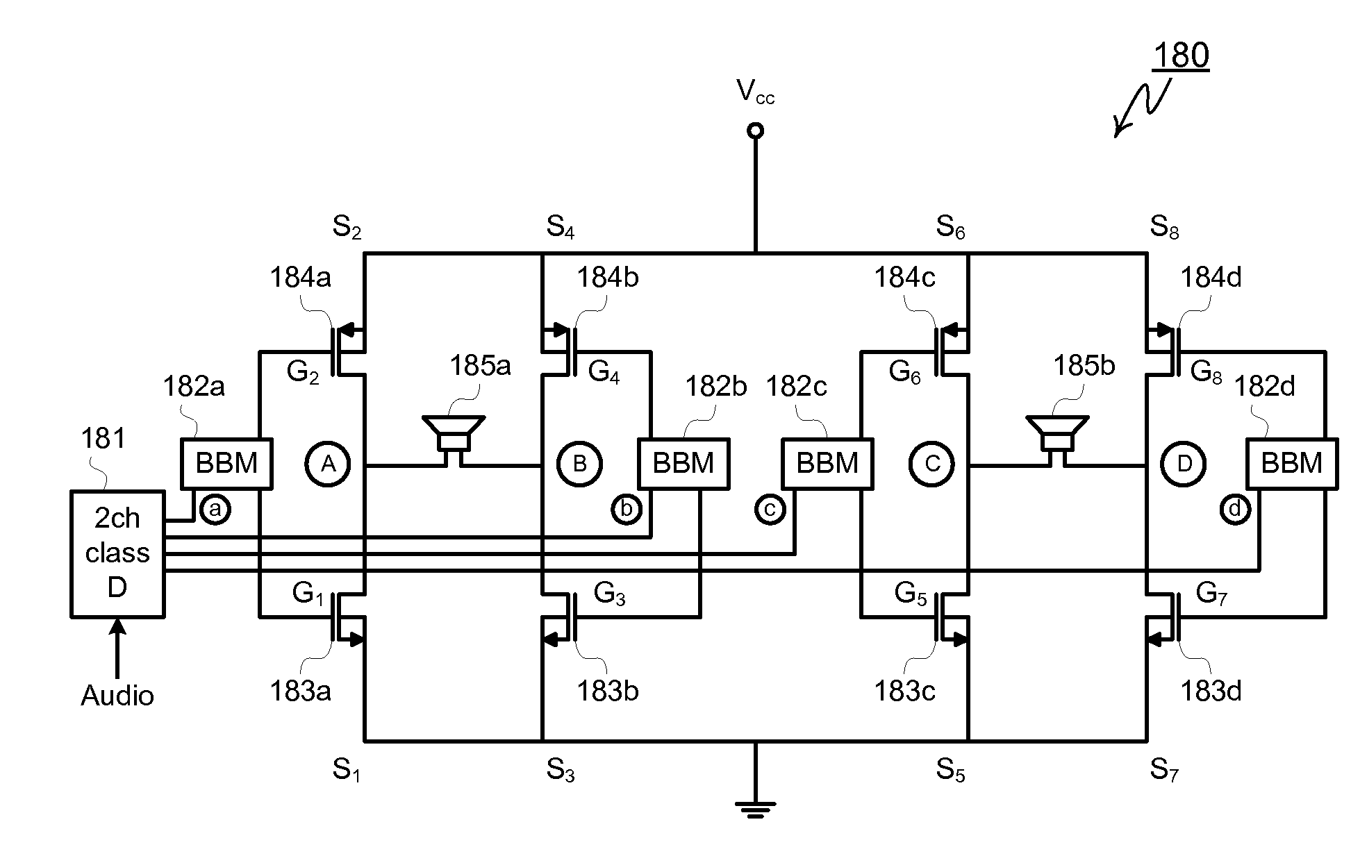
[0094]FIG. 4 illustrates a schematic representation of stereo class-D audio system 180 comprising four complementary half-bridge outputs A, B, C and D with a common class D audio signal processor 181. Each complementary half bridge comprises P-channel high-side device 184A through 184D, low-side N-channel 183A through 183D, and break-before-make (BBM) buffer 182A through 182D, to produce outputs A through D respectively. All N-channel DMOS 183 share a common ground-connected source and have separate drain connected outputs. Similarly, All P-channel DMOS 184 share a common Vcc-connected source and hav...


PUM


Abstract

A stereo class-D audio system includes a first die including four monolithically integrated NMOS high-side devices and a second a second die including four monolithically integrated PMOS low-side devices. The audio system also includes a set of electrical contacts for connecting the high and low-side devices to components within the a stereo class-D audio system, the set of electrical contacts including at least one supply contact for connecting the drains of the high-side devices to a supply voltage (Vcc) and at least one ground contact for connecting the drains of the low-side devices to ground, the electrical contacts also including respective contacts for each source of the high and low-side devices allowing the source of each high-side device to be connected to the source of a respective low-side device to form two H-bridge circuits.

Description

BACKGROUND OF THE INVENTION[0001]High fidelity audio amplification using linear amplification suffers from poor efficiency, excess heating and reduced reliability of power electronic components, and the need for heavy and bulky heat sinking. In portable applications, poor efficiency also leads to shorter and generally unacceptable battery life.[0002]High fidelity linear amplification using class-A amplifiers offers the least distortion but requires its power transistors to continuously carry current and dissipate power. Class B amplifiers introduces a dead-band in the circuit operation where neither transistor conducts but at the expense of increased distortion. Class-AB amplifiers attempt a compromise, but still sacrifice audio quality for efficiency and current consumption.[0003]With the advent of power MOSFETs, a new type of audio amplification with higher efficiency became possible using class-D amplification methods. Class-D amplifiers operate by driving the speaker digitally u...

Claims


Application Information

Patent Timeline
Patent Type & Authority Applications(United States)
IPC IPC(8): H03F3/217
CPCH01L23/3677H01L23/49575H01L2924/1305H01L2224/49111H01L2224/48247H01L2224/48139H01L2224/48137H01L24/49H01L24/48H01L24/45H01L27/092H01L29/407H01L29/42372H01L29/7811H01L29/7813H01L2223/6644H01L2224/45124H01L2224/45144H01L2924/01014H01L2924/0105H01L2924/01078H01L2924/01079H01L2924/13091H01L2924/14H01L2924/19041H03F1/0205H03F3/2171H03F3/2173H03F3/68H03F2200/03H01L2924/01019H01L2924/01013H01L2924/01028H03F3/185H01L2924/10253H01L2924/00014H01L2924/00H01L2924/15747H01L2924/181H01L2924/12035H01L2224/05554H01L2224/0603H01L2224/48464H01L2924/00012H01L2224/85399H01L2224/05599H01L29/7802H03F2200/351
Inventor WILLIAMS, RICHARD K.
Owner ADVANCED ANALOGIC TECHNOLOGIES INCORPORATED
Why Eureka
Try Eureka