Check patentability & draft patents in minutes with Patsnap Eureka AI!

Semiconductor device and method of manufacturing the same

a technology of semiconductors and semiconductors, applied in the field of semiconductor devices, can solve the problems of rising costs of sj structures, and achieve the effect of low cost and low on-resistan

Active Publication Date: 2009-04-21
NISSAN MOTOR CO LTD
View PDF15 Cites 4 Cited by
  • Summary
  • Abstract
  • Description
  • Claims
  • Application Information

AI Technical Summary

Benefits of technology

[0006]An object of the invention is to provide a semiconductor device capable of realizing a switching element having low on-resistance at a low cost, and a method of manufacturing a semiconductor device.

Problems solved by technology

Thus, the SJ structure had a problem of rising costs.

Method used


Image

  • Semiconductor device and method of manufacturing the same
  • Semiconductor device and method of manufacturing the same
  • Semiconductor device and method of manufacturing the same

Examples


first embodiment

[0012](Configuration)

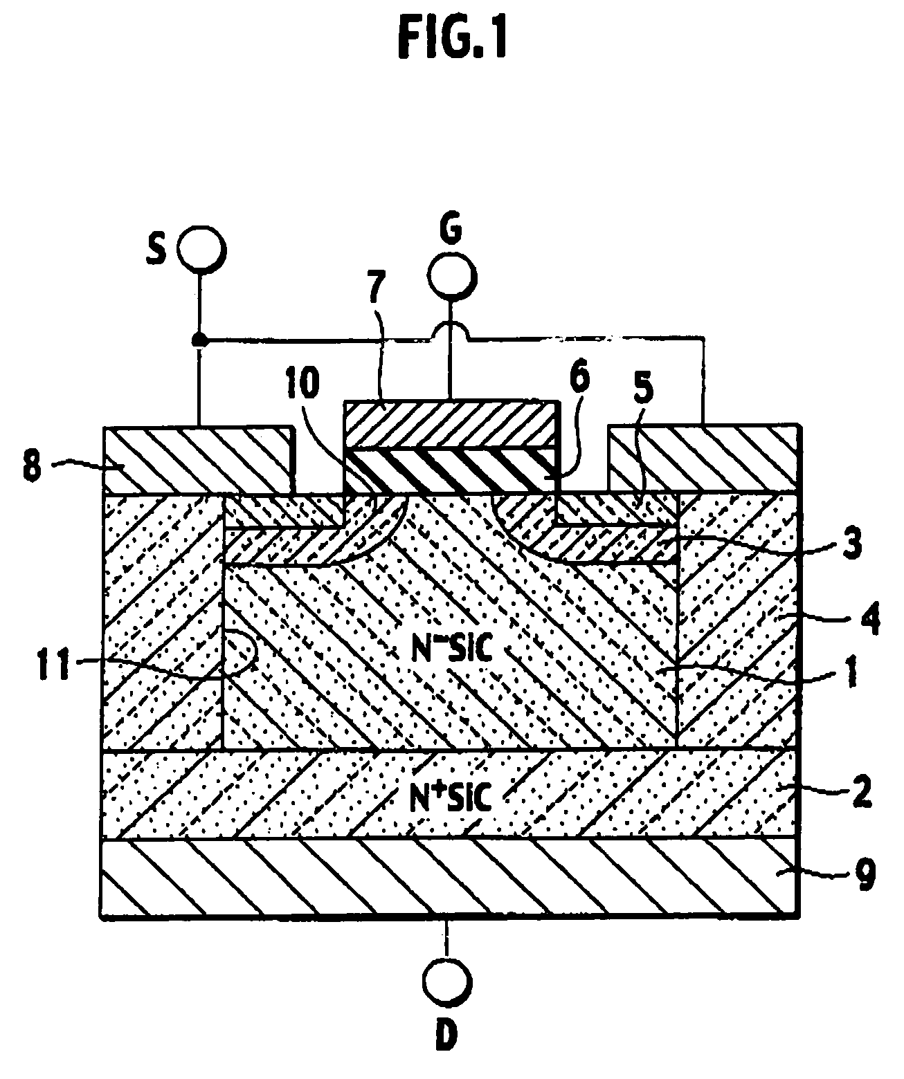
[0013]A first embodiment of the invention will be described with reference to FIG. 1. FIG. 1 is a sectional view showing a structure of an element portion of a semiconductor device according to the first embodiment of the present invention.

[0014]A configuration shown in FIG. 1 will be explained. A drain region 1 made of n-type SiC (silicon carbide) epitaxially grown is formed on an n+ type SiC substrate 2. A power MOSFET is formed on a first main surface of the n-type SiC drain region 1. A polytype of the SiC can be 4H, 6H, 3C, or others. Moreover, the SiC may be replaced by GaN (gallium nitride) or diamond, which is a wide band gap material excellent for use in a power device.

[0015]The power MOSFET used as a switching mechanism may be replaced by a switching mechanism of other switching devices. For example, a JFET (unction FET), a MESFET (metal-semiconductor FET), a bipolar transistor, or a switching mechanism utilizing a heterojunction, which is disclosed in ...

second embodiment

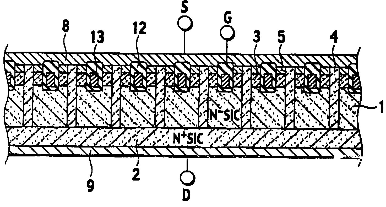
[0027]A second embodiment of the present invention will be described with reference to FIG. 2. FIG. 2 is a sectional view showing a structure of an element portion of a semiconductor device according to the second embodiment of the present invention.

[0028]In the second embodiment, the switching mechanism is applied to a U-gate (trench gate) power MOSFET. In FIG. 2, reference numerals 12 and 13 denote a gate insulating film and a U-gate electrode, respectively.

[0029]The first embodiment has been described by referring to the sectional structure in which two base cells face each other, In FIG. 2 showing the second embodiment, there is illustrated a wide range of the sectional structure in a way that a plurality of columnar hetero-semiconductor regions 4 made of p+ type polysilicon are arranged. The other configurations and the basic operations, functions and effects of the second embodiment are equivalent to those of the first embodiment. Specifically, the second embodiment facilitate...


PUM


Abstract

A semiconductor device of the invention includes a first conductive type semiconductor base substrate; and a switching mechanism which is formed on a first main surface of the semiconductor base substrate and switches ON / OFF of a current. In the semiconductor base substrate, a plurality of columnar hetero-semiconductor regions are formed at spaced intervals within the semiconductor substrate, and the hetero-semiconductor regions are made of a semiconductor material having a different band gap from the semiconductor substrate and extend between the first main surface and a second main surface opposite to the first main surface.

Description

BACKGROUND OF THE INVENTION[0001]The present invention relates to a semiconductor device and a method of manufacturing the same.[0002]Earlier techniques include a so-called superjunction (SJ) power MOSFET (metal oxide semiconductor field effect transistor) described in “Proceedings of 2004 International Symposium Power Semiconductor Devices & ICs, Kitakyushu, p. 459-462,” for example.[0003]The SJ-MOSFET can exceed a limit of theoretical performance determined by an Si (silicon) material, although Si is used as the material of the SJ-MOSFET. Moreover, in the SJ-MOSFET, p and n impurity regions are formed in a sandwich arrangement in a drift region of a body portion. In this structure, a depletion layer is extended in a horizontal direction, and thereby it is possible to simultaneously deplete the whole drift region, which has not been possible with earlier structures. Therefore, the structure can achieve a higher impurity concentration in a p-type region and lower on-resistance as co...

Claims


Application Information

Patent Timeline
Patent Type & Authority Patents(United States)
IPC IPC(8): H01L31/0328
CPCH01L29/0634H01L29/66068H01L29/66712H01L29/66734H01L29/7802H01L29/7813H01L29/8083H01L29/1608H01L29/2003
Inventor SHIMOIDA, YOSHIOHOSHI, MASAKATSUHAYASHI, TETSUYATANAKA, HIDEAKI
Owner NISSAN MOTOR CO LTD
Features
  • R&D
  • Intellectual Property
  • Life Sciences
  • Materials
  • Tech Scout
  • Unparalleled Data Quality
  • Higher Quality Content
  • 60% Fewer Hallucinations
Learn More