Photo apparatus and method

a technology applied in the field of photo apparatus and method, can solve the problem of reducing the entire operation rate, and achieve the effect of enhancing the yield

Active Publication Date: 2009-05-26
LG DISPLAY CO LTD
View PDF4 Cites 19 Cited by
  • Summary
  • Abstract
  • Description
  • Claims
  • Application Information

AI Technical Summary

Benefits of technology

[0037]An advantage of the present invention is to provide a photo apparatus and method to enhance the yield by minimizing an entire layout of photo process line.
[0038]Additional features and advantages of the invention will be set forth in part in the description which follows, and in part will be apparent from the description, or may be learned by practice of the invention. The objectives and other advantages of the invention will be realized and attained by the structure particularly pointed out in the written description and claims hereof as well as the appended drawings.
[0039]To achieve these and other advantages and in accordance with the purpose of the invention, as embodied and broadly described herein, a photo process apparatus including: a loading / unloading unit that loads and unloads a substrate; a coating line that coats photoresist on the substrate; an exposure line that exposes the photoresist coated on the substrate; a development line that develops the exposed substrate; and a transferring line that temporarily stores the substrate coated with the photoresist and loads the substrate coated with the photoresist to the exposure line and temporarily stores the exposed substrate and loads the exposed substrate to the development line.
[0040]In another aspect of the present invention, a photo process apparatus including: a plurality of photo-process lines arranged in parallel, each photo-process line including a loading / unloading unit that loads or unloads a substrate, a coating line that coats photoresist on the substrate, an exposure line that exposes the photoresist coated on the substrate, and a development line that develops the exposed substrate; and a transferring line that transfers the substrate to the coating line, the exposure line, and the development line in each photo-process line according to the processing state of the photo-process line.
[0041]In another aspect of the present invention, a photo process method including: loading a substrate; coating a photoresist on the loaded substrate; temporarily storing the substrate coated with the photoresist; receiving the temporarily stored substrate, and exposing the substrate coated with the photoresist; temporarily storing the exposed substrate; receiving the temporarily stored substrate, and developing the exposed substrate; and unloading the developed substrate.
[0042]In another aspect of the present invention, a photo process method that includes a plurality of photo-process lines arranged in parallel, each photo-process line including a loading / unloading unit that loads or unloads a substrate, a coating line that coats photoresist on the substrate, an exposure line that exposes the photoresist coated on the substrate, and a development line that develops the exposed substrate, including: loading the substrates onto each coating line so as to coat the photoresist on each substrate; temporarily storing the substrates coated in each coating line by using a transferring line that transfers the substrate to the coating line, the exposure line and the development line; exposing the photoresist coated on the substrate by loading the substrate onto the exposure line for each photo-process line that requires the coated substrate through the transferring line; temporarily storing the exposed substrate from each exposure line by using the transferring line; developing the exposed substrate by loading the exposed substrate onto the development line for each photo-process line through the transferring line; and unloading the substrate using the loading / unloading unit.

Problems solved by technology

If there are problems in any one unit of the photo apparatus, the entire operation rate decreases.

Method used


Image

  • Photo apparatus and method
  • Photo apparatus and method
  • Photo apparatus and method

Examples


Embodiment Construction

[0049]Reference will now be made in detail to an embodiment of the present invention, example of which is illustrated in the accompanying drawings. Wherever possible, the same reference numbers will be used throughout the drawings to refer to the same or like parts.

[0050]Hereinafter, a photo apparatus and method according to the present invention will be explained with reference to the accompanying drawings.

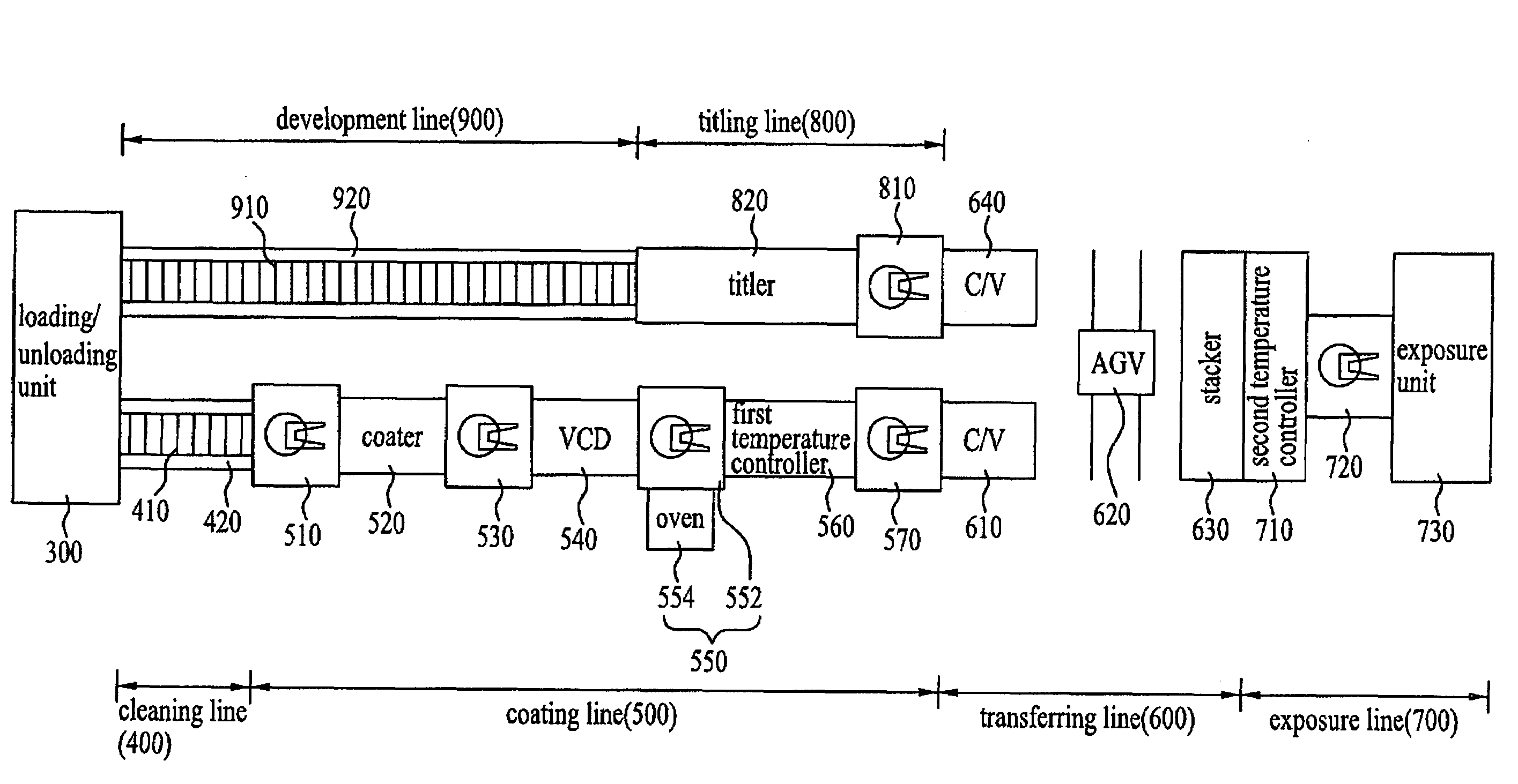
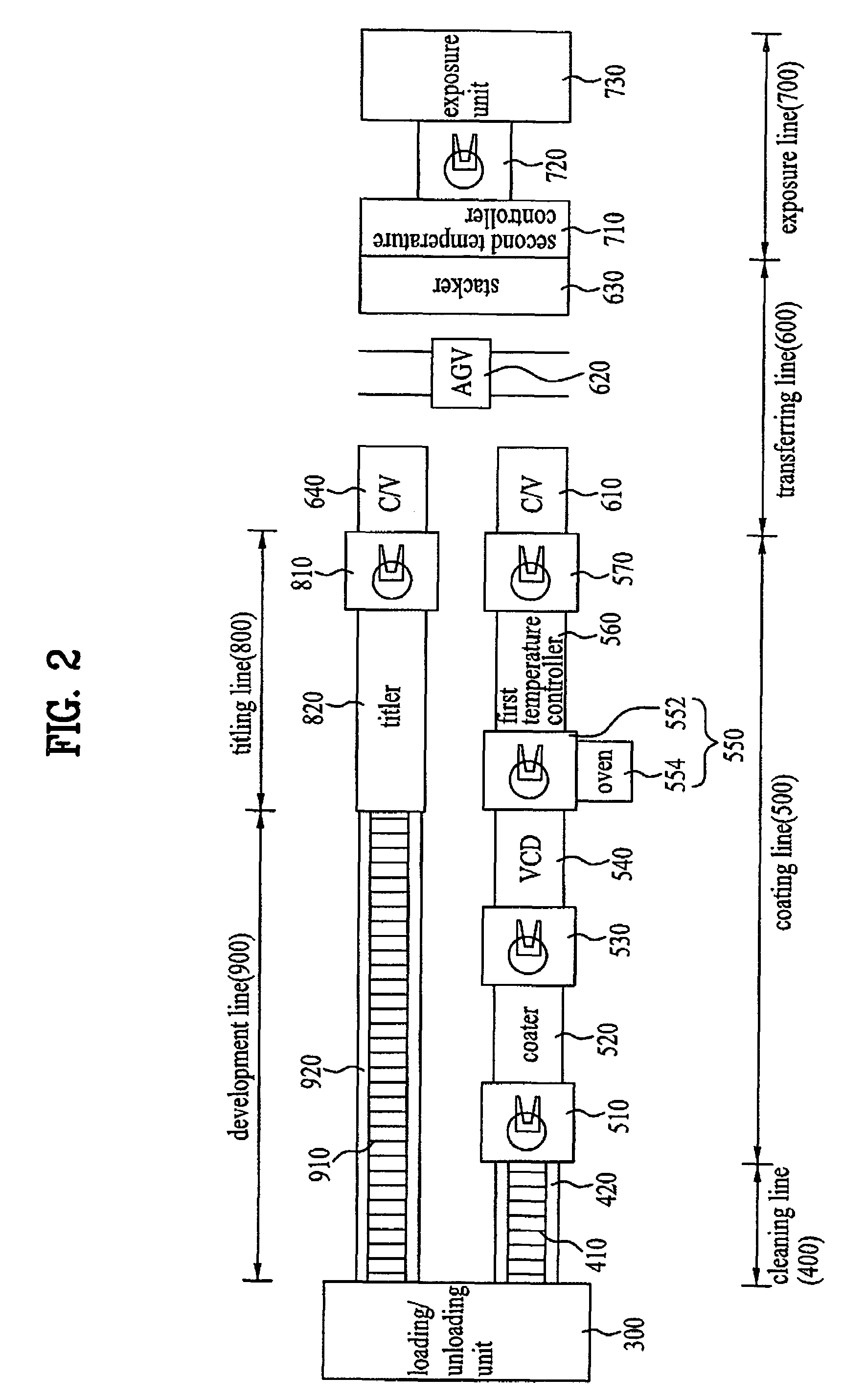
[0051]FIG. 2 is a layout schematically illustrating a photo apparatus according to one preferred embodiment of the present invention.

[0052]Referring to FIG. 2, the photo apparatus according to one preferred embodiment of the present invention includes: a loading / unloading unit 300 that loads or unloads a substrate; a cleaning line 400 that cleans the substrate; a coating line 500 that coats the cleaned substrate with photoresist; an exposure line 700 that exposes the photoresist coated onto the substrate; a titling line 800 that forms an identification code in the exposed substra...


PUM


Abstract

A photo process apparatus including: a loading / unloading unit that loads and unloads a substrate; a coating line that coats photoresist on the substrate; an exposure line that exposes the photoresist coated on the substrate; a development line that develops the exposed substrate; and a transferring line that temporarily stores the substrate coated with the photoresist and loads the substrate coated with the photoresist to the exposure line and temporarily stores the exposed substrate and loads the exposed substrate to the development line.

Description

[0001]This application claims the benefit of Korean Patent Application No. P2006-50468, filed on Jun. 5, 2006, which is hereby incorporated by reference as if fully set forth herein.BACKGROUND OF THE INVENTION[0002]1. Field of the Invention[0003]The present invention relates to a photo apparatus and method, and more particularly, to a photo apparatus and method to enhance yield by minimizing the entire layout of photo process line.[0004]2. Discussion of the Related Art[0005]Generally, a photo process is used for patterning a substrate when fabricating semiconductor devices, flat display devices, etc. The photo process includes coating a photoresist on a substrate, exposing the photoresist coated onto the substrate, and developing the exposed substrate. When the exposing the photoresist, the coated photoresist is selectively exposed.[0006]FIG. 1 is a layout schematically illustrating a related art photo apparatus.[0007]As shown in FIG. 1, the related art photo apparatus is provided w...

Claims


Application Information

Patent Timeline
Patent Type & Authority Patents(United States)
IPC IPC(8): G03D5/00G03B27/32
CPCH01L21/67173H01L21/67207H01L21/67225H01L21/67276H01L21/67727G03F7/16G03F7/30B65G49/07G03F7/0035H01L21/027G03F7/70808
Inventor KIM, YONG HUNSEO, JIN WOO
Owner LG DISPLAY CO LTD
Why Eureka
Try Eureka