Method and system for improving dielectric film quality for void free gap fill

a dielectric film and void-free technology, applied in the field of dielectric film quality improvement, can solve the problems of large height-to-width ratio gap and trench, fabrication problems, and difficulty in completely filling the gap and trench in these structures without creating, so as to improve the quality of dielectric film morphologically and increase the density

Active Publication Date: 2009-06-02
APPLIED MATERIALS INC
View PDF68 Cites 527 Cited by
  • Summary
  • Abstract
  • Description
  • Claims
  • Application Information

AI Technical Summary

Benefits of technology

[0009]The present invention is directed to semiconductor thin film process techniques. Methods and system are described for improving quality of the dielectric film morphologically adapted over various device structures. More particularly, embodiments of the invention provide methods and systems of forming silicon oxide film with increased density to achieve void free gap fill for trenches having a high aspect ratio. For example, the invention is applied to form high quality silicon oxide films for filling narrow STI trenches, among other applications.

Problems solved by technology

However, the vertical heights of the STI trenches normally do not decrease as fast as their horizontal widths, resulting in gaps and trenches with larger ratios of height to width (i.e., higher the aspect ratios).
While the ability to make device structures with increasing aspect ratios allows more of the structures (e.g., transistors, capacitors, diodes, etc.) to be packed onto the same surface area of a semiconductor chip substrate, it has also created fabrication problems.
One of these problems is the difficulty of completely filling the gaps and trenches in these structures without creating a void or seam during the filling process.
As aspect ratios increase, it becomes more difficult to fill deep narrow trenches without creating a void or seam in the dielectric material that fills the trench.
Voids and seams in a dielectric layer cause problems both during semiconductor device fabrication and in the finished devices.
This results in unpredictable and inconsistent post-deposition processing of the layer, such as non-uniform etching, polishing, annealing, etc.
This can result in erratic and inferior device performance due to electrical crosstalk, charge leakage, and in some instances, shorting within the device, among other problems.
A more conformal deposition can reduce material buildup at the top of the trench and the chance of dielectric material prematurely sealing off the top of the trench to form a void (a problem sometimes referred to as “breadloafing”).
Unfortunately however, slowing the deposition rate also means increasing the deposition time, which reduces processing efficiency and production rates.
However, increasing the flowability of an silicon oxide dielectric material by such conventional SOG films often results in an as-deposited film with low film density caused by residual carbon species and unreacted silanol groups.
However, the high-temperature annealing used to remove residual carbon species and OH groups may also cause a considerable degree of volumetric shrinkage of film.

Method used


Image

  • Method and system for improving dielectric film quality for void free gap fill
  • Method and system for improving dielectric film quality for void free gap fill
  • Method and system for improving dielectric film quality for void free gap fill

Examples


Embodiment Construction

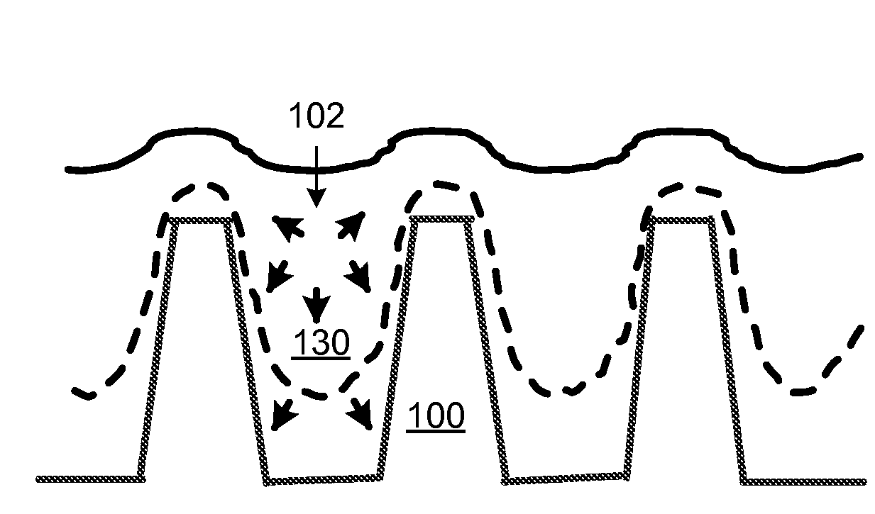
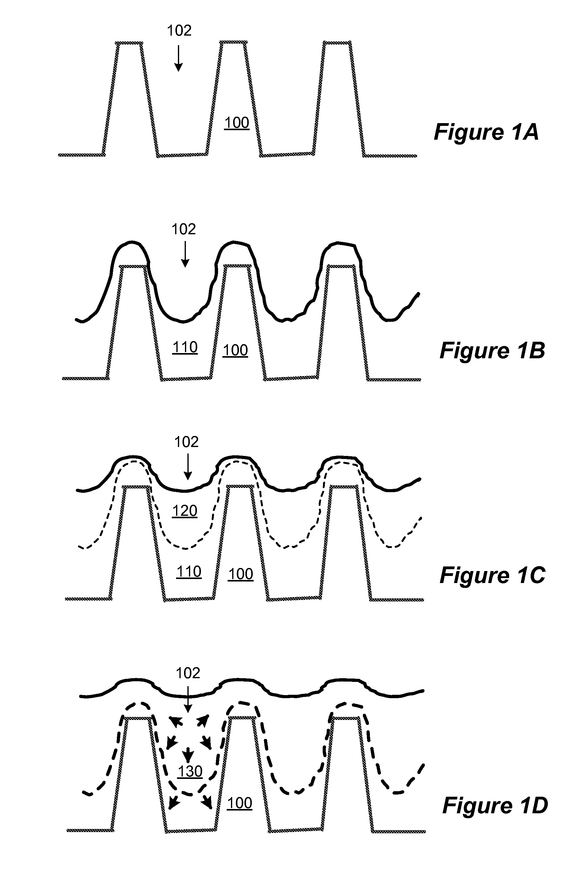
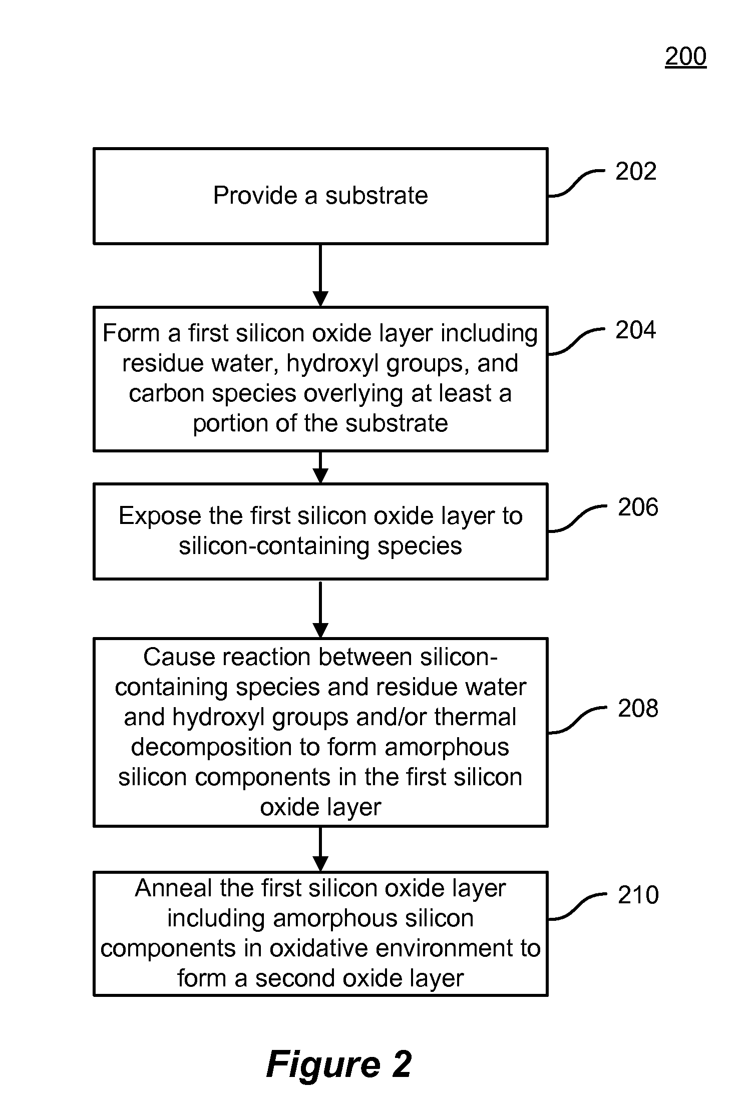
[0021]Methods and systems are described for improving quality of the dielectric film morphologically adapted over various semiconductor device structures. More particularly, embodiments of the invention provide methods and system of forming silicon oxide film with increased density to achieve void free gap fill for trenches with a high aspect ratio. For example, the invention may be applied to form high quality silicon oxide films for filling narrow STI trenches, among other applications.

[0022]Flowable silicon dioxide films deposited by chemical vapor deposition techniques from silicon-containing precursors (e.g., organosilicates) and remote plasma generated atomic oxygen have been applied to STI applications. The as-deposited flowable oxide films may initially have relatively low film density due in part to ingredients like residual water and carbon species, as well as significant hydroxyl groups. During the deposition of the flowable oxide film or after certain amount of flowable ...


PUM

PropertyMeasurementUnit
temperatureaaaaaaaaaa
pressureaaaaaaaaaa
temperatureaaaaaaaaaa

Abstract

A method of forming a silicon oxide layer on a substrate. The method includes providing a substrate and forming a first silicon oxide layer overlying at least a portion of the substrate, the first silicon oxide layer including residual water, hydroxyl groups, and carbon species. The method further includes exposing the first silicon oxide layer to a plurality of silicon-containing species to form a plurality of amorphous silicon components being partially intermixed with the first silicon oxide layer. Additionally, the method includes annealing the first silicon oxide layer partially intermixed with the plurality of amorphous silicon components in an oxidative environment to form a second silicon oxide layer on the substrate. At least a portion of amorphous silicon components are oxidized to become part of the second silicon oxide layer and unreacted residual hydroxyl groups and carbon species in the second silicon oxide layer are substantially removed.

Description

CROSS-REFERENCES TO RELATED APPLICATIONS[0001]This application is related to co-assigned U.S. Patent Application No. 60 / 803,493 by Ingle et al, and titled “CHEMICAL VAPOR DEPOSITION OF HIGH QUALITY FLOW-LIKE SILICON DIOXIDE USING A SILICON CONTAINING PRECURSOR AND ATOMIC OXYGEN”, filed on May 30, 2006. This application is also related to co-assigned U.S. Non-provisional patent application Ser. No. 11 / 845,445 by Mallick et al, and titled “CURING METHODS FOR SILICON DIOXIDE THIN FILMS DEPOSITED FROM ALKOXYSILANE PRECURSOR WITH HARP II PROCESS”, also filed Aug. 27, 2007. This application is additionally related to co-assigned U.S. patent application Ser. No. 11 / 876,538, by Mallick et al, and titled “HIGH QUALITY SILICON OXIDE FILMS BY REMOTE PLASMA CVD FROM DISILANE PRECURSORS”, also filed Oct. 22, 2007 The entire contents of all the above applications is hereby incorporated by reference for all purposes.FIELD OF THE INVENTION[0002]The present invention is directed to semiconductor thi...

Claims


Application Information

Patent Timeline
Patent Type & Authority Patents(United States)
IPC IPC(8): H01L21/469H01L21/31
CPCC23C16/045C23C16/24C23C16/401C23C16/56H01L21/02126H01L21/02164H01L21/02274H01L21/0228H01L21/02337H01L21/0234H01L21/31612H01L21/76837
Inventor MALLICK, ABHIJIT BASUMUNRO, JEFFREY C.WANG, LINLINNEMANI, SRINIVAS D.ZHENG, YIYUAN, ZHENGLUBOMIRSKY, DIMITRYYIEH, ELLIE Y.
Owner APPLIED MATERIALS INC
Why Eureka
Try Eureka