Pixel structures of color filter substrate, active device array substrate and liquid crystal display panel

a color filter substrate and active device array technology, applied in non-linear optics, instruments, optics, etc., can solve the problems of low yield, complicated processing, poor spatial utilization, etc., and achieve the effect of low production yield and wide viewing angle characteristics

Active Publication Date: 2009-06-02
AU OPTRONICS CORP
View PDF3 Cites 13 Cited by
  • Summary
  • Abstract
  • Description
  • Claims
  • Application Information

AI Technical Summary

Benefits of technology

[0008]Accordingly, the present invention is directed to pixel structures of a color filter substrate, an active device array substrate and a liquid crystal display panel having wide viewing angle characteristics and resolving complicated processing procedures and low production yield problems.
[0023]In the present invention, the viewing angle of the liquid crystal display is enhanced by adjusting the liquid crystal capacitance, the storage capacitance and the gate-drain capacitance. Since there is no need to provide the additional process of fabricating the alignment protrusions or slits, the liquid crystal display can have better production yield and lower production cost. Furthermore, different voltages can be applied to the electrode patterns in a single pixel structure to enhance the viewing angle by designing of the electrode patterns on the color filter substrate.

Problems solved by technology

However, the poor spatial utilization and high power consumption of the CRT often cause many problems.
However, regardless of the types of technologies, the disadvantages are complicated processing and low yield.
Although the twisted nematic liquid crystal display added wide viewing films can produce better viewing characteristics, the design of the liquid crystal display panel is directly limited by the wide viewing film.
Moreover, the protrusions and slits also make it difficult to reduce the thickness of the liquid crystal display panel, and the disadvantages of lower the transmission rate of the back light source and light leakage in a darkened state are also existed.
Hence, the cost of producing the liquid crystal display panel is increased while the production yield drops.

Method used


Image

  • Pixel structures of color filter substrate, active device array substrate and liquid crystal display panel
  • Pixel structures of color filter substrate, active device array substrate and liquid crystal display panel
  • Pixel structures of color filter substrate, active device array substrate and liquid crystal display panel

Examples


Embodiment Construction

[0034]Reference will now be made in detail to the present preferred embodiments of the invention, examples of which are illustrated in the accompanying drawings. Wherever possible, the same reference numbers are used in the drawings and the description to refer to the same or like parts.

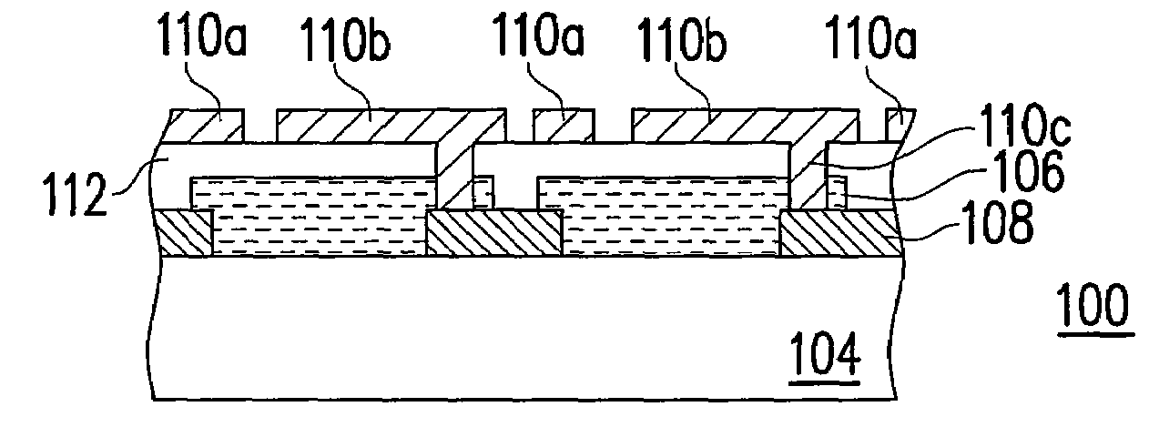
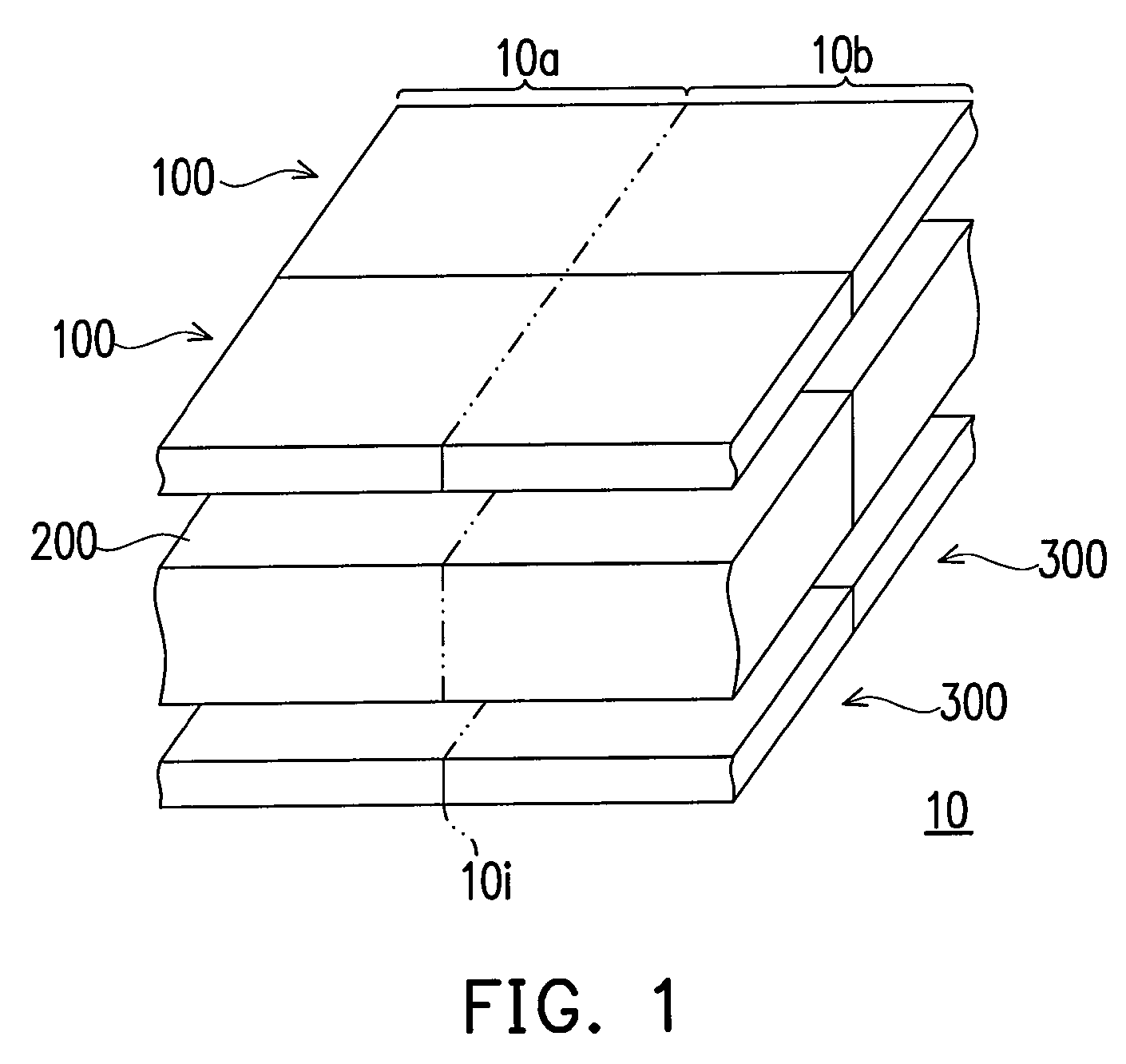
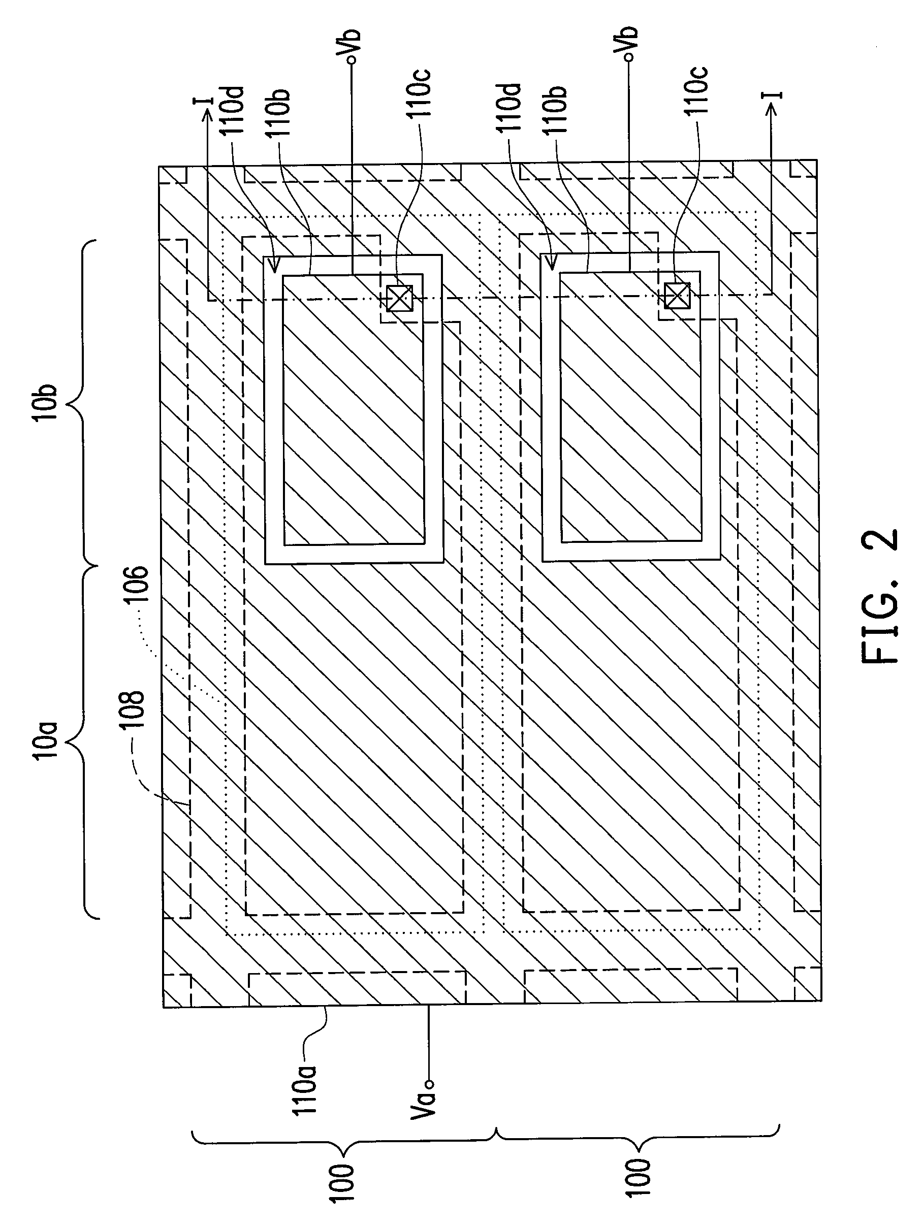
[0035]In order to provide the liquid crystal display with wide viewing angle characteristics, each pixel structure of the color filter substrate, the active device array substrate and the liquid crystal display panel of the present invention is divided into two areas. For the pixel structure of the color filter substrate, the common electrodes in the two areas are electrically connected to different voltage input terminals. For the pixel structure of the active device array substrate, these two areas have different pixel electrode areas, gate-drain capacitances and / or storage capacitances. Therefore, a single pixel structure can align the liquid crystal molecules to two different angles of alignment ...


PUM

PropertyMeasurementUnit
areaaaaaaaaaaa
voltageaaaaaaaaaa
input voltageaaaaaaaaaa

Abstract

Pixel structures of a color filter substrate, an active device array substrate and a liquid crystal display panel are provided. The pixel structure of the color filter substrate includes a first and second electrode patterns electrically connected to different voltage input terminals. The pixel structure of the active device array substrate includes a first and second pixel electrodes, a first and second gate-drain capacitances and a first and second storage capacitances. The areas of the first and the second pixel electrodes are different, the first and the second gate-drain capacitances are different, and the first and the second storage capacitances are different. In addition, the pixel structure of the liquid crystal display panel includes the pixel structure of the color filter substrate the pixel structure, the active device array substrate and a liquid crystal layer therebetween.

Description

CROSS-REFERENCE TO RELATED APPLICATION[0001]This application claims the priority benefit of Taiwan application serial no. 95141635, filed Nov. 10, 2006. All disclosure of the Taiwan application is incorporated herein by reference.BACKGROUND OF THE INVENTION[0002]1. Field of the Invention[0003]The present invention relates to a structure of a liquid crystal display, and more particularly to a pixel structures of a color filter substrate, an active device array substrate and a liquid crystal display panel.[0004]2. Description of Related Art[0005]The rapid development of multi-media in our society is mostly the result of a series of breakthroughs in the fabrication of semiconductor devices and display devices. In the past, cathode ray tubes (CRTs) have been the dominant displays in the market due to their good display quality and economy. However, the poor spatial utilization and high power consumption of the CRT often cause many problems. Therefore, thin film transistor liquid crystal...

Claims


Application Information

Patent Timeline
Patent Type & Authority Patents(United States)
IPC IPC(8): G02F1/136
CPCG02F1/134309G02F1/133512G02F2001/134345G02F2001/136231G02F1/134345G02F1/136231
Inventor LU, AN-HSU
Owner AU OPTRONICS CORP
Why Eureka
Try Eureka