Solid state imaging device and method for manufacturing the same

a technology of solid-state imaging and manufacturing methods, applied in the direction of instruments, optical elements, optical waveguide light guides, etc., can solve problems that are still unsolved, and achieve the effect of improving light sensitivity

Inactive Publication Date: 2009-06-16
COLLABO INNOVATIONS INC
View PDF3 Cites 0 Cited by
  • Summary
  • Abstract
  • Description
  • Claims
  • Application Information

AI Technical Summary

Benefits of technology

[0011]Although the CCD solid state imaging device shown in FIG. 9 improves in sensitivity to light, there has been a problem still unsolved. Specifically, light incident obliquely on the CCD solid state imaging device (hereinafter referred to as oblique light) and light coming through a gap between adjacent microlenses (hereinafter referred to as a lens gap) enter adjacent pixels other than the target pixel, thereby causing color mixing.
[0014]Under these circumstances, the present invention has been achieved. An object of the present invention is to provide a CCD solid state imaging device which makes it possible to prevent color mixing due to the entrance of oblique light and light coming through the lens gap and to reduce the variations in sensitivity to light between the pixels.
[0016]In the solid state imaging device according to a first aspect of the present invention, the second optical waveguides are formed in addition to the first optical waveguides. With this structure, light coming through the lens gap and oblique light are confined in the second optical waveguides. This makes it possible to attenuate the intensities of the lights and prevent the entrance of them into pixels adjacent to the target pixel. As a result, color mixing is prevented and the pixels are less likely to vary in sensitivity to light.
[0023]By the method according to the first aspect of the present invention, the second optical waveguides are formed in addition to the first optical waveguides. In the solid state imaging device manufactured by the method, light coming through the lens gap and oblique light are confined in the second optical waveguides. This makes it possible to attenuate the intensities of the lights and prevent the entrance of them into pixels adjacent to the target pixel. Thus, the solid state imaging device prevents color mixing and reduces variations in sensitivity to light between the pixels.
[0025]As to the method according to the first aspect of the present invention, in the step (d), the second insulating film may be formed to fill the first openings and the second openings and cover the surface of the first insulating film and then part of the second insulating film positioned above the first insulating film may be removed. In this case, the second insulating film fills both of the first and second openings, thereby reducing the height of protrusions to be generated on the insulating film. This makes the following planarization step easy.

Problems solved by technology

Although the CCD solid state imaging device shown in FIG. 9 improves in sensitivity to light, there has been a problem still unsolved.

Method used


Image

  • Solid state imaging device and method for manufacturing the same
  • Solid state imaging device and method for manufacturing the same
  • Solid state imaging device and method for manufacturing the same

Examples


first embodiment

[0037]Hereinafter, explanation of a CCD solid state imaging device according to a first embodiment of the present invention is provided with reference to the drawings. As pixels in the CCD solid state imaging device of the present embodiment are provided in the same arrangement as those of the conventional device shown in FIG. 7, detailed explanation and graphic representation thereof are omitted.

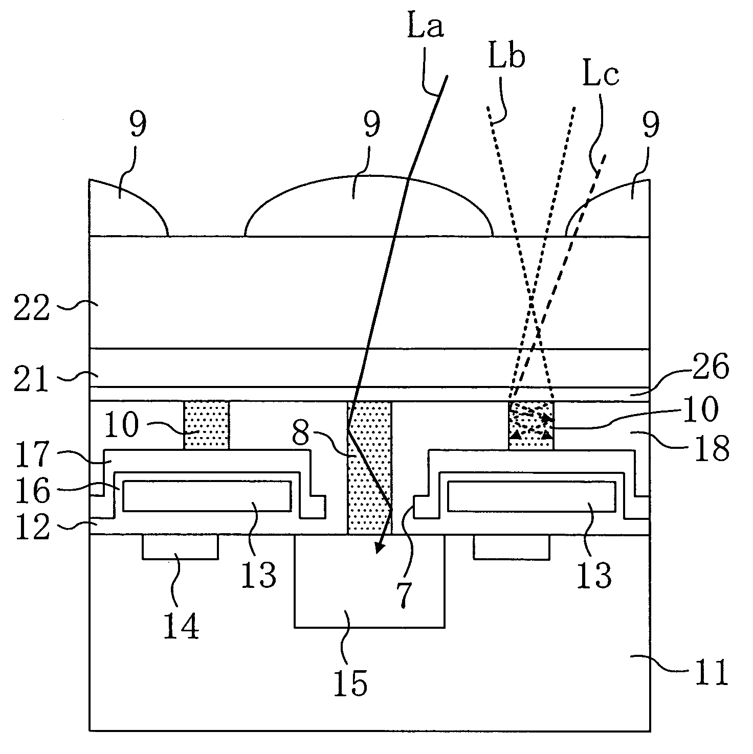
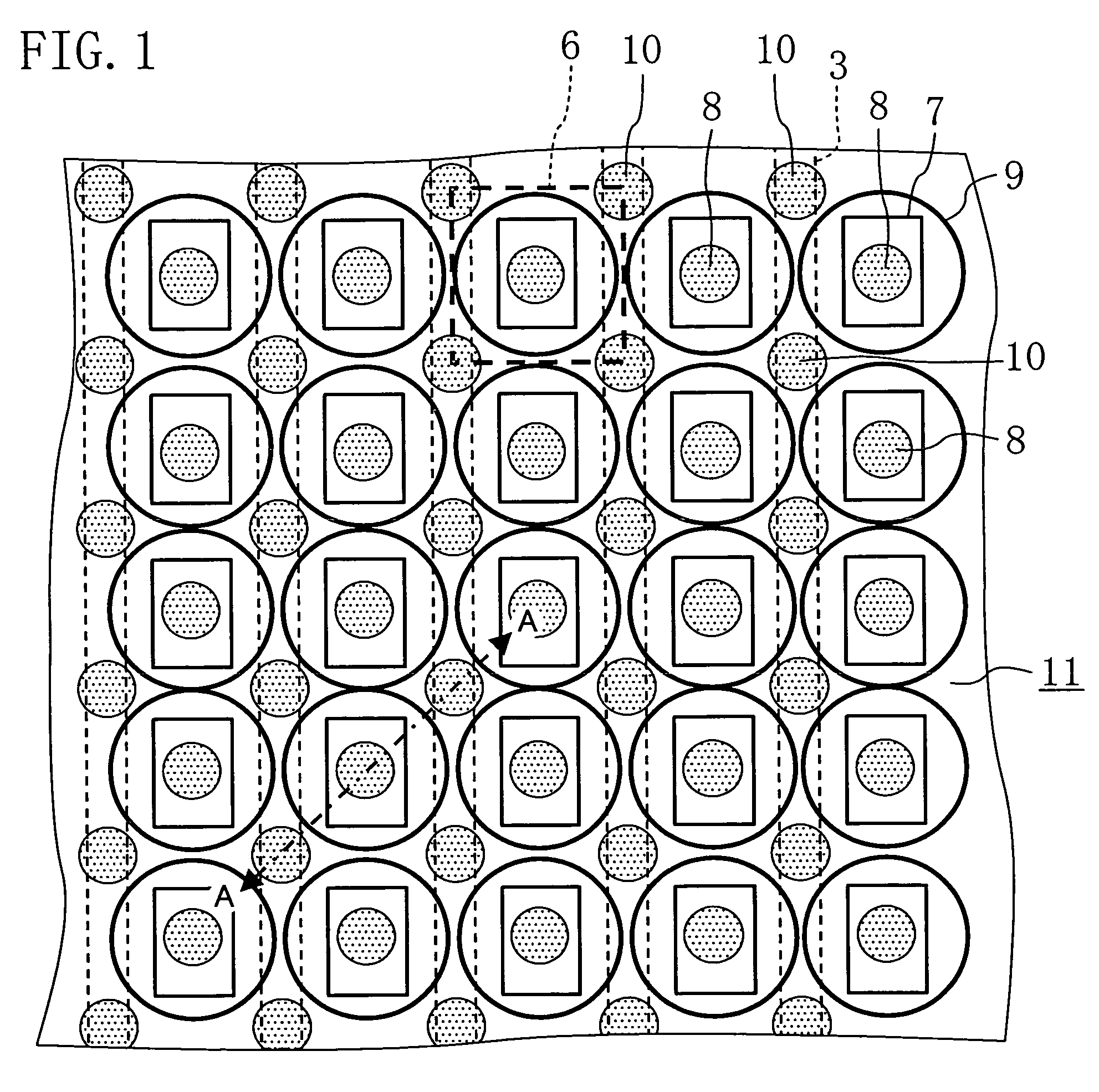
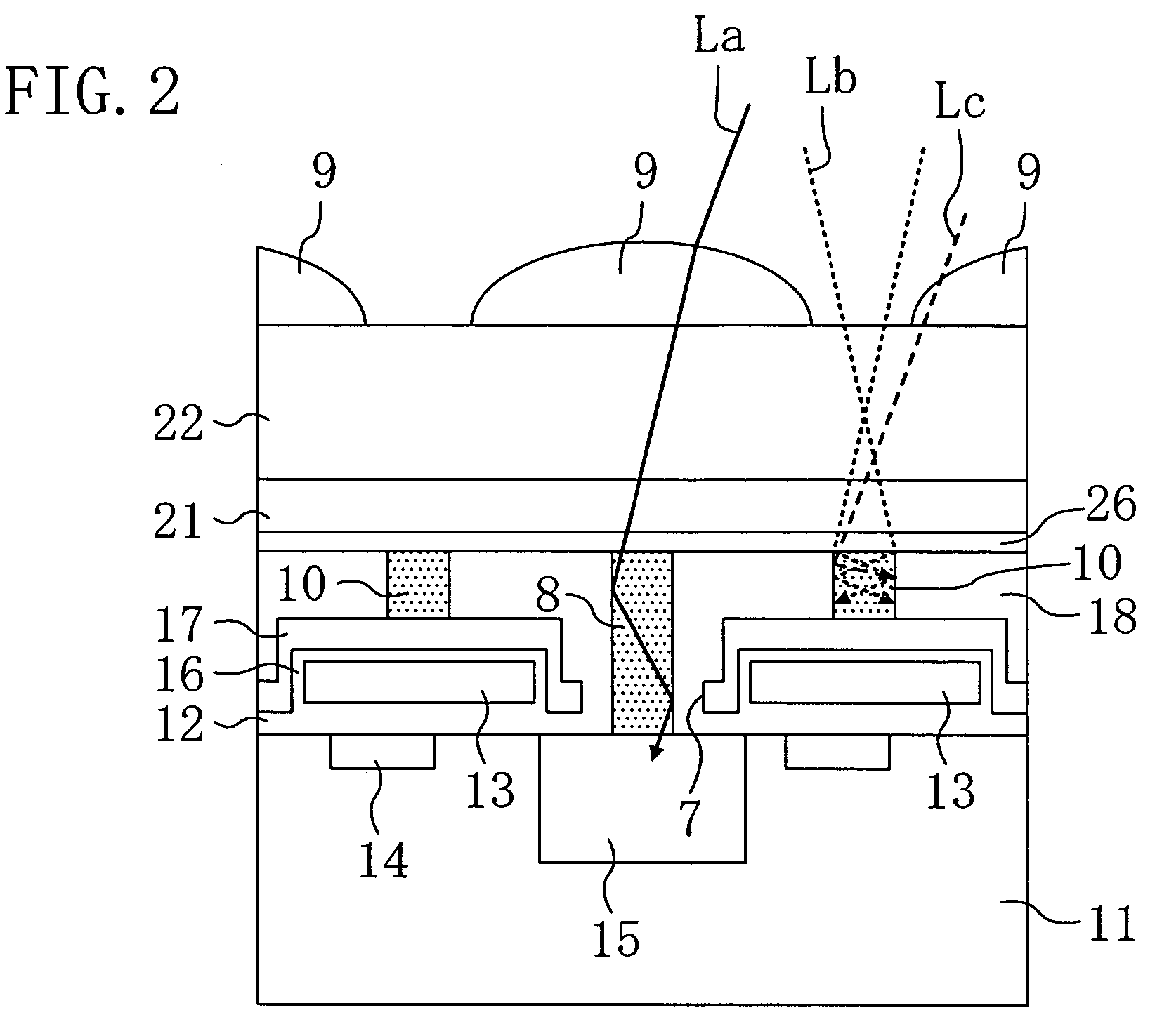
[0038]FIG. 1 is a plan view illustrating an enlargement of part of the CCD solid state imaging device according to the first embodiment and FIG. 2 is a sectional view taken along the line II-II shown in FIG. 1.

[0039]As shown in FIG. 1, the CCD solid state imaging device of the present embodiment includes a semiconductor substrate 11 on which vertical CCDs 3, openings 7 and on-chip microlenses 9 are provided. First optical waveguides 8 are formed in the openings 7 such that each of the first optical waveguides 8 is positioned at the center of the diagonal line of the opening 7. Second optica...

second embodiment

[0055]FIG. 4 is a plan view illustrating an enlargement of part of a CCD solid state imaging device according to a second embodiment. In the solid state imaging device of the present embodiment, light absorbers 25 are provided below the second optical waveguides 10, i.e., between the second optical waveguides 10 and the light shield film 17. This structure makes it possible to reduce re-reflection of light to a further extent. Other structures and effects of the present embodiment are the same as those of the first embodiment and therefore the explanation is omitted.

Other Embodiments

[0056]In the first and second embodiments described above, explanation is made with the CCD solid state imaging device taken as an example. However, the solid state imaging device of the present invention may be a MOS solid state imaging device.

[0057]In the first and second embodiments described above, the second optical waveguides 10 are round-shaped when viewed in plan (FIG. 1). However, the planar sha...


PUM


Abstract

A plurality of light receiving elements are arranged in a matrix with uniform space therebetween in a light receiving region defined on a semiconductor substrate. A plurality of read-out electrodes are formed on the semiconductor substrate in an arrangement corresponding to the light receiving elements to read charges generated by the light receiving elements, a light shield film having openings positioned above the light receiving elements is formed to cover the read-out electrodes, first optical waveguides are formed in the openings above the light receiving elements and second optical waveguides are formed on the light shield film. The second optical waveguides are in the form of dots, stripes or a grid when viewed in plan.

Description

BACKGROUND OF THE INVENTION[0001]1. Field of the Invention[0002]The present invention relates to a solid state imaging device and a method for manufacturing the same. In particular, it relates to a solid state imaging device including a plurality of light receiving elements arranged in a matrix and a method for manufacturing the same.[0003]2. Description of Related Art[0004]In recent years, there has been an increasing demand for solid state imaging devices as imaging devices for digital still cameras and video cameras. Further, in the field of mobile devices such as cellular phones, camera-equipped ones are highly demanded. From this aspect, the demand for the solid state imaging devices has been expanding. Aiming at higher quality images, the number of pixels tends to increase year after year. As the increase in pixel count involves the need of decreasing pixel area, further improvement in light gathering power has been demanded.[0005]Now, referring to FIGS. 7 to 9, explanation of...

Claims


Application Information

Patent Timeline
Patent Type & Authority Patents(United States)
IPC IPC(8): G02B6/12
CPCH01L27/1462H01L27/14623H01L27/14685H01L27/1463H01L27/14806
Inventor KURIYAMA, TOSHIHIROTOMOZAWA, ATSUSHI
Owner COLLABO INNOVATIONS INC
Why Eureka
Try Eureka