Quantum dot optoelectronic devices with nanoscale epitaxial lateral overgrowth and methods of manufacture

an optoelectronic device and quantum dot technology, applied in the field of optoelectronic devices, can solve the problems of not being able to use leds for general lighting applications, efficient device performance, etc., and achieve the effect of facilitating nanoscale epitaxial lateral overgrowth (nelog) and higher efficiency

Inactive Publication Date: 2009-06-30
NORTH CAROLINA AT CHARLOTTE THE UNIV OF +1
View PDF19 Cites 24 Cited by
  • Summary
  • Abstract
  • Description
  • Claims
  • Application Information

AI Technical Summary

Benefits of technology

[0013]The present invention provides for optoelectronic devices that incorporate quantum dots as the electroluminescent layer in an inorganic wide-bandgap double heterostructure. Examples of such devices include quantum dot light emitting diodes (QD-LED), laser diodes, photodetectors and the like. The quantum dots serve as the optically active component of the device and, in multilayer quantum dot embodiments, facilitate nanoscale epitaxial lateral overgrowth (NELO) in heterostructures having non-lattice matched substrates. The quantum dots in such devices will be electrically pumped and exhibit electroluminescence, as opposed to being optically pumped and exhibiting photoluminescence. There is no inherent “Stokes loss” in electroluminescence, thus the devices of the present invention have higher efficiency entitlement than optically pumped quantum dot devices. Devices resulting from the present invention are capable of providing deep green visible light, as well as, any other color in the visible spectrum, including white light by blending the size of the dots and controlling manufacturing processes. In addition to the devices, the present invention also provides for novel means of manufacturing optoelectronic devices that incorporate quantum dots.
[0014]In the present invention the semiconductor quantum dots are disposed between two semiconductor electrodes, where the electrode bandgap is larger than that of the dots themselves, thus facilitating (1) direct electrical excitation of the quantum dots, potentially eliminating “Stokes losses” and (2) recombination of electron-hole pairs in a quantum confined environment, maximizing quantum efficiency. The present invention is superior to placing quantum dots on top of an LED, because such an optically excited approach results in “Stokes loss” every time a photon is downconverted. The present invention is also superior to placing the quantum dots between organic electrodes because organic electrodes are fundamentally less stable than the inorganic semiconductor electrodes proposed in the present invention.
[0025]Thus, the present invention provides for optoelectronic devices that incorporate quantum dots as the electroluminescent layer in an inorganic wide-bandgap heterostructure. The quantum dots serve as the optically active component of the device and, in multilayer quantum dot embodiments, facilitate nanoscale epitaxial lateral overgrowth (NELOG) in heterostructures having non-lattice matched substrates. The quantum dots in such devices will be electrically pumped and exhibit electroluminescence, as opposed to being optically pumped and exhibiting photoluminescence. There is no inherent “Stokes loss” in electroluminescence thus the devices of the present invention have higher efficiency than optically pumped quantum dot devices. Devices resulting from the present invention are capable of providing deep green visible light, as well as, any other color in the visible spectrum, including white light by blending the size of the dots and controlling manufacturing processes.

Problems solved by technology

Until recently, it was not possible to use LEDs for general lighting applications, because general “white” lighting requires a blending of photons with several different energies, e.g. red, green, and blue, and the technology did not exist to make bright blue emitters.
For wavelengths shorter than 380 nm, the relative lack of indium in the InGaN alloy does not allow for efficient light emitting devices and beyond 520 nm the InGaN nanostructure does not result in efficient device performance.

Method used


Image

  • Quantum dot optoelectronic devices with nanoscale epitaxial lateral overgrowth and methods of manufacture
  • Quantum dot optoelectronic devices with nanoscale epitaxial lateral overgrowth and methods of manufacture
  • Quantum dot optoelectronic devices with nanoscale epitaxial lateral overgrowth and methods of manufacture

Examples


Embodiment Construction

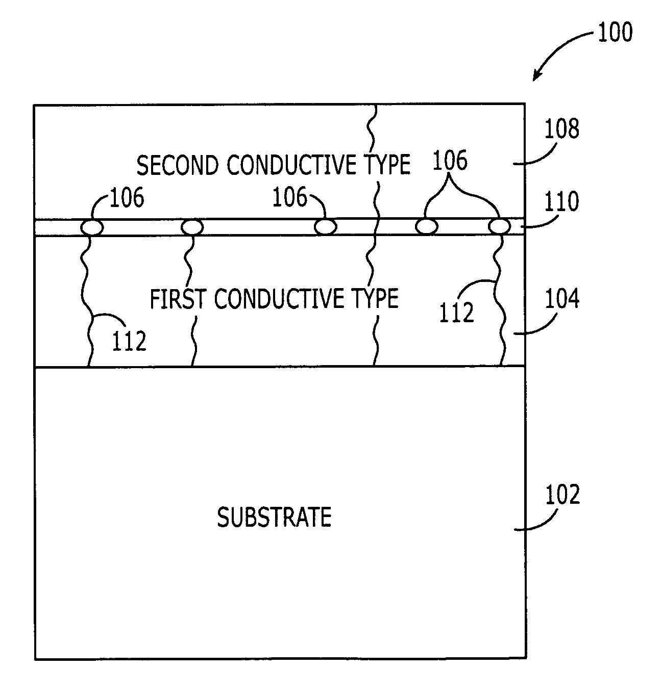
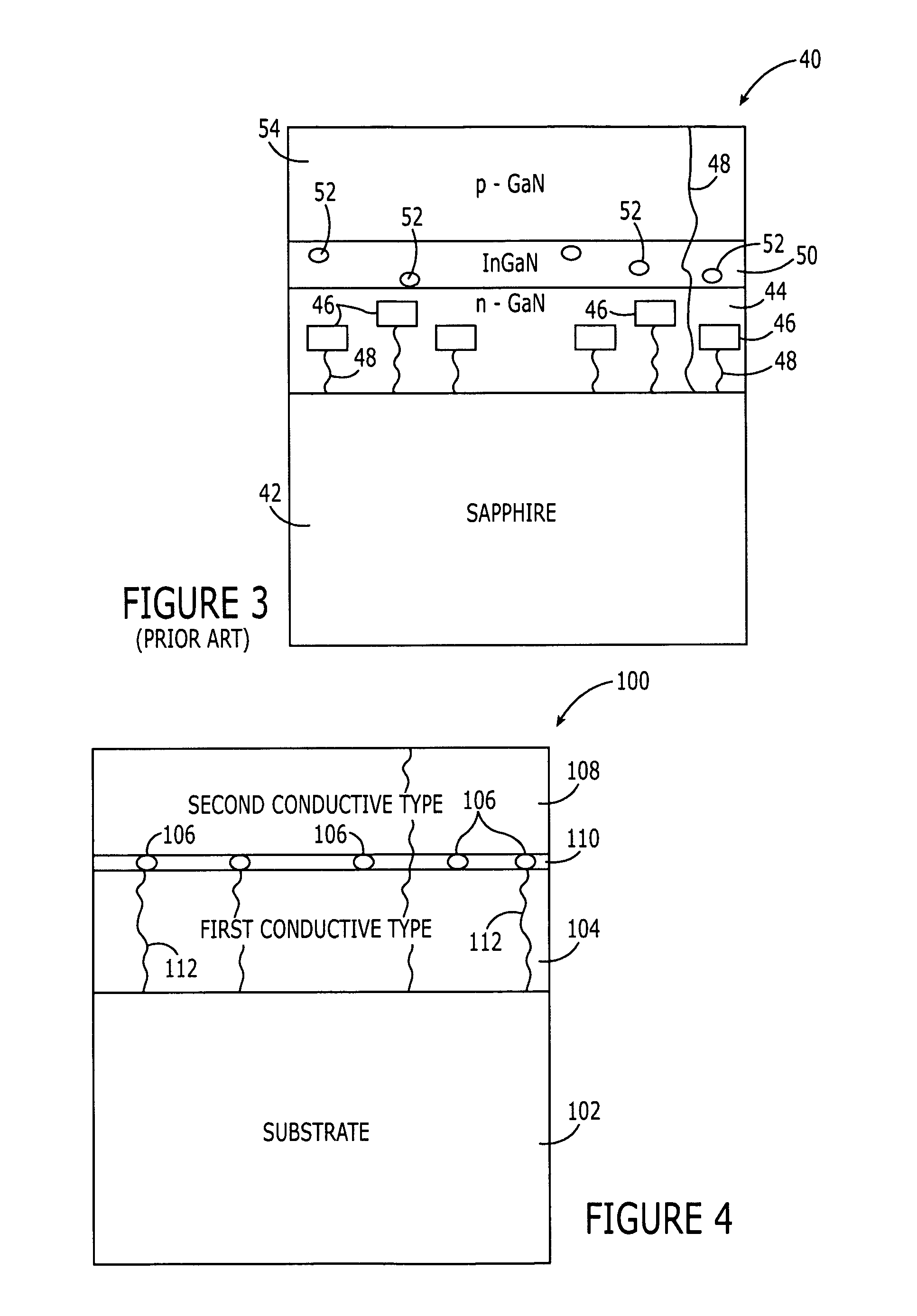
[0036]The present inventions now will be described more fully hereinafter with reference to the accompanying drawings, in which some, but not all embodiments of the invention are shown. Indeed, these inventions may be embodied in many different forms and should not be construed as limited to the embodiments set forth herein; rather, these embodiments are provided so that this disclosure will satisfy applicable legal requirements. Like numbers refer to like elements throughout.

[0037]The present invention provides for optoelectronic devices that incorporate quantum dots as the electroluminescent layer in an inorganic wide-bandgap heterostructure. Examples of such devices include quantum dot light emitting diodes (QD-LED), laser diodes, photodetectors and the like. The quantum dots serve as the optically active component of the device and, in multilayer quantum dot embodiments, facilitate nanoscale epitaxial lateral overgrowth (NELOG) in heterostructures having non-lattice matched subs...


PUM


Abstract

Optoelectronic devices are provided that incorporate quantum dots as the electroluminescent layer in an inorganic wide-bandgap heterostructure. The quantum dots serve as the optically active component of the device and, in multilayer quantum dot embodiments, facilitate nanoscale epitaxial lateral overgrowth (NELOG) in heterostructures having non-lattice matched substrates. The quantum dots in such devices will be electrically pumped and exhibit electroluminescence, as opposed to being optically pumped and exhibiting photoluminescence. There is no inherent “Stokes loss” in electroluminescence thus the devices of the present invention have potentially higher efficiency than optically pumped quantum dot devices. Devices resulting from the present invention are capable of providing deep green visible light, as well as, any other color in the visible spectrum, including white light by blending different sizes and compositions of the dots and controlling manufacturing processes.

Description

CROSS-REFERENCE TO RELATED APPLICATIONS[0001]This application claims the benefit of U.S. Provisional Application No. 60 / 500,273, filed Sep. 5, 2003, entitled Quantu Dot Optoelectronic Devices (Q-DOD) with Nanoscale Epitaxial Lateral Overgrowth (NELOG), the contents of which are incorporated herein by reference in its entirety.FIELD OF THE INVENTION[0002]The present invention relates to optoelectronic devices and, more specifically, to devices incorporating quantum dots that (1) serve as active layers and (2) facilitate nanoscale epitaxial lateral overgrowth and (3) facilitate methods for manufacture of optoelectronic devices.BACKGROUND OF THE INVENTION[0003]Semiconductor Light Emitting Diodes, commonly referred to as LEDs, were introduced in the 1960's when visible red light was produced using gallium arsenide phosphide (GaAsP) on a GaAs substrate (Ref. N. Holonyak Jr. and S. F. Bevacqua, “Coherent (Visible) Light Emission from Ga(As1−xPx) Junctions,” Appl. Phys. Lett., vol. 1, pp. ...

Claims


Application Information

Patent Timeline
Patent Type & Authority Patents(United States)
IPC IPC(8): H01L29/205H01L29/12H01L33/06H01L33/08H01S5/323H01S5/34
CPCB82Y10/00B82Y20/00H01L29/127H01L33/06H01S5/32341H01S5/341H01L33/08H01S5/3412H01S2304/12Y10S977/817Y10S977/816
Inventor STOKES, EDWARD B.HASAN, MOHAMED-ALISUNDERASAN, KAMALPAGAN, JENNIFER G.
Owner NORTH CAROLINA AT CHARLOTTE THE UNIV OF
Why Eureka
Try Eureka