
Method for the selective removal of an unsilicided metal

a metal and unsilicide technology, applied in the field of integrated circuits, can solve the problems of no silicidation at the spacer and isolating, aqua regia is a chemical solution that is highly corrosive and unstable, and the solution is barely compatible with industrial use, and achieves the effect of metal germanide dissolution

Inactive Publication Date: 2009-08-04
STMICROELECTRONICS (CROLLES 2) SAS
View PDF7 Cites 0 Cited by
  • Summary
  • Abstract
  • Description
  • Claims
  • Application Information

AI Technical Summary

Benefits of technology

The invention proposes a method for easily silicidating new metals while being compatible with conventional metals like nickel. The method involves depositing a metal layer on a silicon-containing region, forming a metal silicide, and then removing the residue metal. The residue metal is converted to an alloy containing the germanide of the metal and dissolved in a chemical solution. This method can be carried out using conventional chemical solutions commonly used in microelectronics. The invention also provides a method for selectively removing an unsilicided metal with respect to its silicide using a chemical solution. The method can be implemented by depositing a material comprising germanium and annealing it at a temperature between 100 and 600° C. The silicon-containing region can be any region of a transistor, such as a source, drain, or gate region.

Problems solved by technology

However, there is no silicidation at the spacers and the isolating zone, which generally consist of silicon oxide or silicon nitride.
However, aqua regia also attacks platinum silicide, and is therefore not selective with respect to platinum alone.
In addition, aqua regia is a chemical solution that is highly corrosive and unstable over time.
It is therefore a solution barely compatible with use in an industrial environment.
In the case of iridium, there is no known chemistry that allows it to be dissolved while leaving the silicide behind.
These constraints greatly limit the choice of chemical solution for the new metals envisaged and, in general, result in highly corrosive solutions that are therefore barely usable in an industrial environment.

Method used


Image

  • Method for the selective removal of an unsilicided metal
  • Method for the selective removal of an unsilicided metal
  • Method for the selective removal of an unsilicided metal

Examples


Embodiment Construction

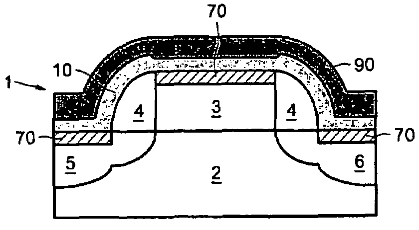
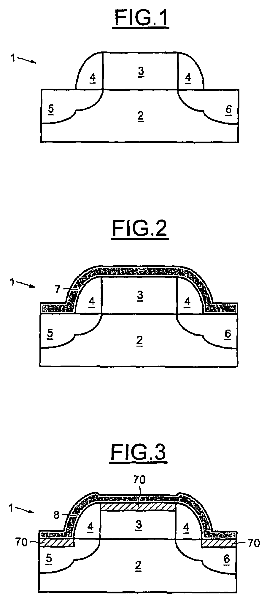
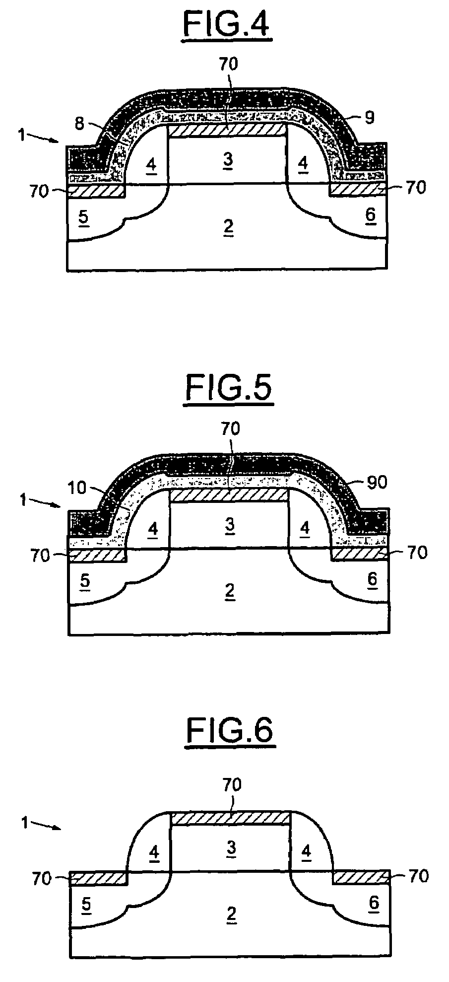
[0029]FIG. 1 shows very schematically a cross section through an integrated circuit 1 comprising a transistor produced on a substrate 2. The transistor comprises a gate 3, spacers 4 placed on either side of the gate 3, a source region 5 and a drain region 6.

[0030]A metal layer 7 is deposited on the surface of the transistor, on top of the source 5, drain 6 and gate 3 regions and on top of the spacers 4. As an example, platinum will be used as the metal. The integrated circuit 1 as shown in FIG. 2 is obtained.

[0031]Next, a silicidation step is carried out. During this step, a metal silicide 70, in the present case platinum silicide, is formed in the source 5, drain 6 and gate 3 regions. However, platinum does not react with the spacers 4, which essentially comprise silicon nitride. The unreacted platinum is on the surface of the transistor and forms in a layer of residue of metal 8 (FIG. 3).

[0032]The next step comprises depositing a second layer 9, comprising germanium, on the transi...


PUM

PropertyMeasurementUnit
temperatureaaaaaaaaaa

Abstract

An integrated circuit is silicided by depositing at least one metal on a silicon-containing region and forming a metal silicide. Residue metal that has not been silicided during the formation of the metal silicide is then removed. The removal of the residue metal involves the conversion of the residue metal to an alloy containing the germanide of said metal with minimal if any adverse affect on the silicide. Next, the alloy is removed, in a manner selective to the silicide, by dissolving the alloy in a chemical solution.

Description

PRIORITY CLAIM[0001]The present application claims priority from French Application for Patent No. 06 00436 filed Jan. 18, 2006, the disclosure of which is hereby incorporated by reference.BACKGROUND OF THE INVENTION[0002]1. Technical Field of the Invention[0003]The present invention relates to integrated circuits, and more particularly to the formation of a metal silicide on an integrated circuit component.[0004]2. Description of Related Art[0005]The production of microelectronic components often includes a step of siliciding part of said component. The siliciding step consists in the formation of a metal silicide on a silicon zone. This step most particularly takes place on surfaces that are used as contact surfaces between the microelectronic component and the connection tracks. Silicidation makes it possible to achieve better conductivity at these surfaces thanks to the silicon / metal alloy thus formed, which has a very low contact resistance.[0006]Silicidation methods are curren...

Claims


Application Information

Patent Timeline
Patent Type & Authority Patents(United States)
IPC IPC(8): H01L21/302H01L21/44H01L21/461H01L21/4763
CPCH01L21/02068H01L21/32134H01L21/28518
Inventor HALIMAOUI, AOMAR
Owner STMICROELECTRONICS (CROLLES 2) SAS
Learn More