Interposer bonding device

a technology of interposer and boding device, which is applied in the direction of semiconductor/solid-state device details, instruments, manufacturing tools, etc., can solve the problems of above-described conventional interposer boding device and the insufficient increase in production efficiency, so as to achieve the working of electronic components continuously and very efficiently

Active Publication Date: 2009-08-25
HALLYS CORP
View PDF113 Cites 5 Cited by
  • Summary
  • Abstract
  • Description
  • Claims
  • Application Information

AI Technical Summary

Benefits of technology

[0005]The present invention has been made in view of the above-described conventional problem and is intended for providing an interposer bonding device with increased production efficiency.
[0006]The present invention provides an interposer bonding device for bonding an interposer to a base circuit sheet, the interposer having a semiconductor chip mounted on a sheet-like chip holding member and having an interposer-side terminal as a connection terminal extending from the semiconductor chip, the base circuit sheet formed from a sheet-like base member and provided with a base-side terminal on a surface thereof, the interposer bonding device including a press anvil that holds the base circuit sheet on which the interposer is laminated, with the interposer-side terminal and the base-side terminal facing each other; and a bonding head that can move relatively with respect to the press anvil, in which the bonding head has a pressing surface that can press a rear surface of the interposer or the base circuit sheet by abutting against the rear surface, the pressing surface being able to scan the rear surface of the interposer or the base circuit sheet according to the relative movement of the bonding head to the press anvil and to press the whole surface of the interposer-side terminal to the base circuit sheet.
[0008]Because of this, in the interposer bonding device of the present invention, for example, it is possible to simultaneously perform a step of conveying a workproduct and supplying the workproduct to the bonding head and a step of pressing and bonding the interposer by use of the bonding head. In addition, it is possible to take out a worked electronic component while performing the step of pressing and bonding the interposer by use of the bonding head. For this reason, according to the interposer bonding device, it is possible to perform the working of the electronic component continuously and very efficiently.

Problems solved by technology

However, the above-described conventional interposer boding device has a problem as given below.
That is, in the above-described bonding device, it is necessary that a step for arranging a workproduct in the press dies, a step for press by use of the press dies, and a step for taking out the workproduct be performed in sequence, and this poses the problem that there is a fear that the production efficiency may not be sufficiently increased.

Method used


Image

  • Interposer bonding device
  • Interposer bonding device
  • Interposer bonding device

Examples


embodiment 1

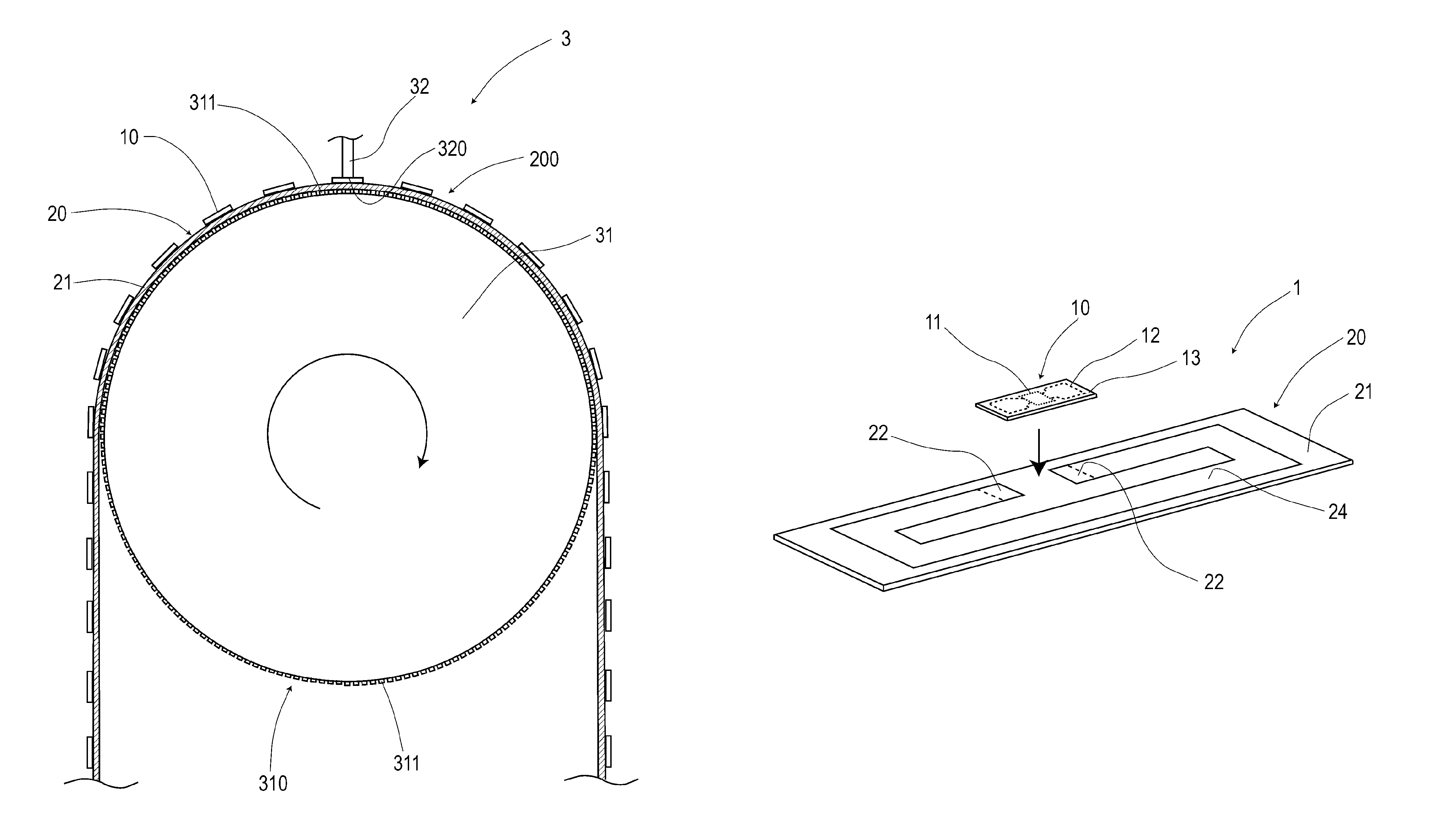
[0051]This embodiment relates to an interposer bonding device 3 for fabricating an electronic component 1 in which an interposer 10 is bonded to a base circuit sheet 20. This embodiment will be described with reference to FIGS. 1 to 9.

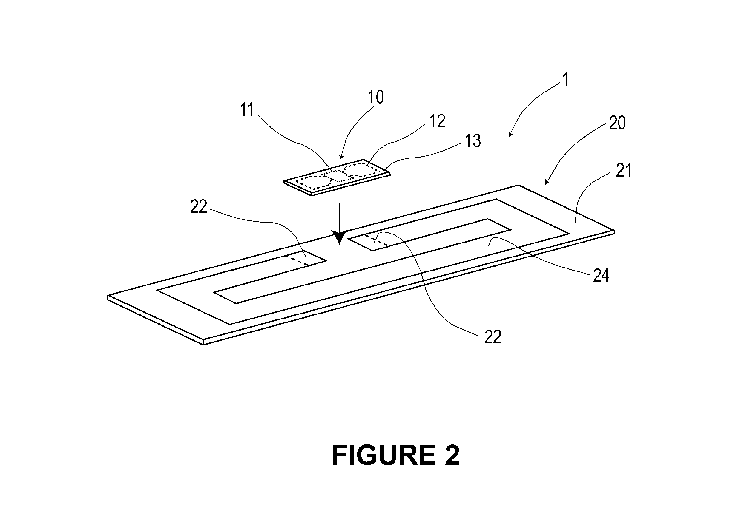
[0052]As shown in FIGS. 1 and 2, the interposer bonding device 3 of this embodiment is intended for bonding an interposer 10 in which a semiconductor chip 11 is mounted on a sheet-like chip holding member 13 and which has an interposer-side terminal 12, which is a connection terminal provided in an extending manner from the semiconductor chip 11, to a base circuit sheet 20 that is formed from a sheet-like base member 21 and is provided, on a surface thereof, with a base-side terminal 22.

[0053]This interposer bonding device 3 has a press anvil 31 that holds the base circuit sheet 20 on which the interposer 10 is laminated, with the interposer-side terminal 12 and the base-side terminal 22 facing each other, and a bonding head 32 that moves relatively wi...

embodiment 2

[0088]In this embodiment, mainly the shapes of the pressing surface 320 of the bonding head 32 and the convex portion 310 of the press anvil 31 are changed on the basis of the interposer bonding device 3 of Embodiment 1. This embodiment will be described with reference to FIGS. 11 to 16.

[0089]In the interposer bonding device 3 of this embodiment, as shown in FIG. 11, the bonding head 32 abuts against the antenna sheet 20 and the press anvil 31 abuts against interposer 10.

[0090]As shown in FIGS. 11 and 12, the bonding head 32 of this embodiment has a pressing surface 320 that is formed so as to correspond to the curved peripheral surface of the press anvil 31. This pressing surface 320 is such that the size thereof which is coincident with the circumferential direction of the press anvil 31 is wider than the interposer 10. Because of this, in the interposer bonding device 3 of this embodiment, it is possible to simultaneously press the whole surface of the interposer-side terminal 12...


PUM

PropertyMeasurementUnit
thickaaaaaaaaaa
thickaaaaaaaaaa
protruding height hdaaaaaaaaaa

Abstract

An interposer bonding device 3 is intended for bonding an interposer 10 having an interposer-side terminal to a base circuit sheet 20 provided with a base-side terminal. The interposer bonding device 3 has a press anvil 31 that holds the base circuit sheet 20 on which the interposer 10 is laminated and a bonding head 32 that moves relatively with respect to the press anvil 31. The bonding head 32 has a pressing surface 320 that presses the rear surface of the interposer by abutting against this surface. The pressing surface 320 scans the rear surface of the interposer 10 by the relative movement of the bonding head 32 with respect to the press anvil 31 and presses the whole surface of the interposer-side terminal 12 toward the base circuit sheet 20.

Description

CROSS-REFERENCE TO RELATED APPLICATIONS[0001]The benefit of priority is claimed to International Application PCT / JP05 / 22220, filed Dec. 3, 2005, the entire contents of which are incorporated by reference herein. The benefit of priority is further claimed to Japanese patent applications 2004-350841 and 2004-351258, both filed Dec. 3, 2004; and the entire contents of both Japanese applications are also incorporated herein by reference.TECHNICAL FIELD[0002]The present invention relates to an electronic component manufacturing apparatus for bonding an interposer on which a semiconductor chip is mounted to a base circuit sheet.RELATED ART[0003]For example, there have been available RF-ID media in which an interposer, in which an IC chip is mounted on a resin film, is laminated on an antenna sheet and bonded thereto. In fabricating such RF-ID media, an interposer may be laminated via an adhesive and an antenna sheet is pressed in the lamination direction thereof. Examples of an interposer...

Claims


Application Information

Patent Timeline
Patent Type & Authority Patents(United States)
IPC IPC(8): B23P19/00
CPCG06K19/07718G06K19/07752H01L24/75H01L24/83H01L24/97G06K19/07749Y10T29/4913H01L2223/6677H01L2924/14H05K3/323H01L23/66H01L24/29H01L24/32H01L2224/2919H01L2224/32225H01L2224/83192H01L2224/83205H01L2224/83385H01L2224/97H01L2924/1421Y10T29/53174Y10T29/53178Y10T29/53187Y10T29/53183H01L2924/07802H01L2224/83H01L2924/00
Inventor NISHIGAWA, RYOICHIAOYAMA, HIROSHI
Owner HALLYS CORP
Why Eureka
Try Eureka