Semiconductor package with electromagnetic shielding capabilities

a technology of electromagnetic shielding and electromagnetic shielding, which is applied in the direction of semiconductor devices, semiconductor/solid-state device details, electrical apparatus, etc., can solve the problems of destructing the zoological balance, adversely affecting human health, and affecting the zoological balance, so as to achieve effective shielding electromagnetic interference, enhance heat dissipation efficiency, and increase engagement strength

Active Publication Date: 2009-08-25
ADVANCED SEMICON ENG INC
View PDF2 Cites 14 Cited by
  • Summary
  • Abstract
  • Description
  • Claims
  • Application Information

AI Technical Summary

Benefits of technology

[0007]An object of the present invention is to provide a semiconductor package having shielding metal balls disposed between and around adjacent dies thereof to effectively shield electromagnetic interference.
[0009]Preferably, the present semiconductor package further includes a heat spreader that is disposed on the semiconductor dies to enhance the heat dissipation efficiency.
[0010]Further, a molding compound is preferably applied between the heat spreader and the upper surface of the substrate to increase the engagement strength between the heat spreader and the substrate.
[0011]Accordingly, the present semiconductor package provides a more effective EMI shielding capability by the employment of a plurality of shielding metal elements disposed between and around the semiconductor dies. Further, the overall vertical height of the present semiconductor package employing these shielding metal elements is not increased while providing such an effective EMI shielding effect. In addition, a heat spreader and a molding compound can be further incorporated into the present semiconductor package to respectively enhance the heat dissipation efficiency and the structural strength of the present semiconductor package.

Problems solved by technology

The electromagnetic waves generated by electrical or electronic devices in operation may interfere with other surrounding electrical or electronic devices, which has adverse influences on the normal operation and the stable signal transmission of these devices.
Further, excessive electromagnetic interference causes electromagnetic contamination, which adversely affects the human health and destructs the zoological balance.
However, with the rapid development of the electrical and electronic industry, it has become more and more difficult to obtain such an electromagnetic compatibility status.
However, mutual electromagnetic interference occurs between the dies in the package, and external electromagnetic signals also interfere with the operation of these dies, which may result in damage of the dies and malfunction of the package incorporating these dies.

Method used


Image

  • Semiconductor package with electromagnetic shielding capabilities
  • Semiconductor package with electromagnetic shielding capabilities
  • Semiconductor package with electromagnetic shielding capabilities

Examples


Embodiment Construction

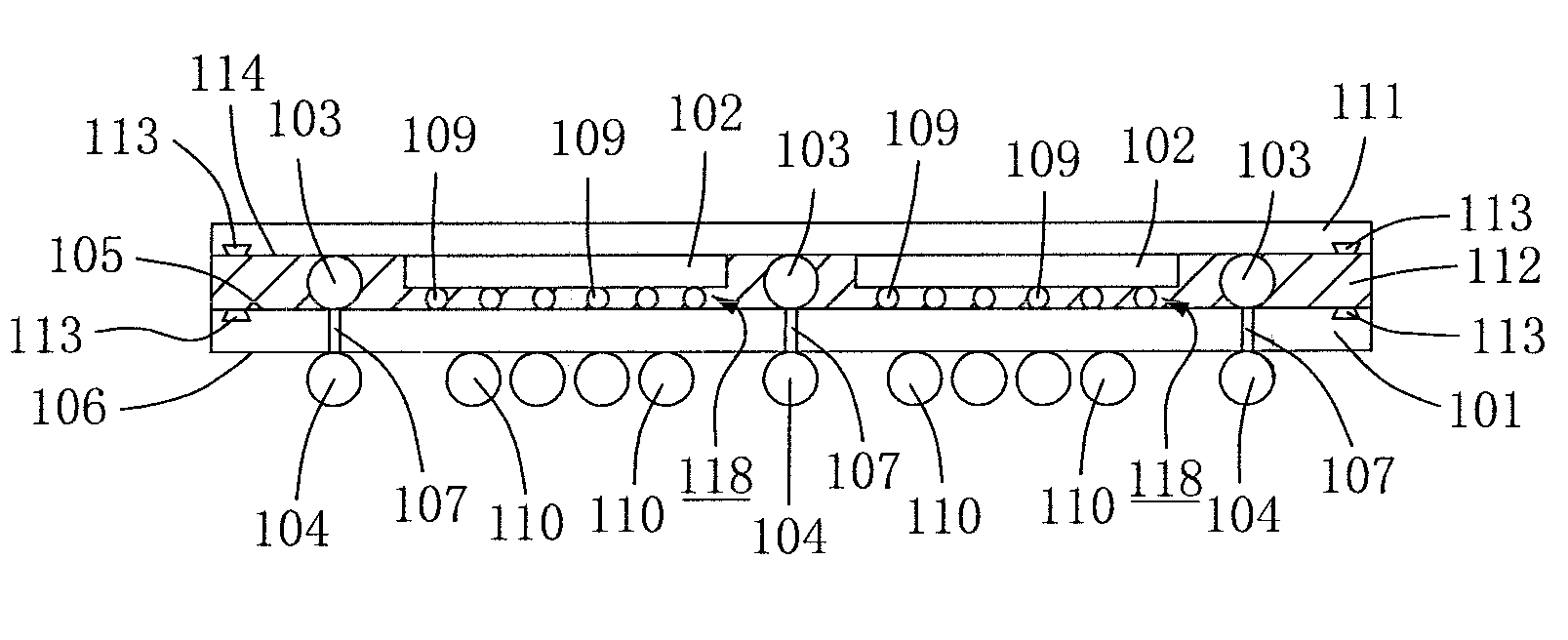
[0016]Referring to FIG. 1, a semiconductor package with electromagnetic shielding capabilities in accordance with a first embodiment of the present invention includes a substrate 101, a plurality of semiconductor dies 102 (two shown for simplicity), a plurality of shielding metal elements 103, a plurality of grounding metal elements 104 and a plurality of conductive metal elements 110. The shielding metal elements 103, the grounding metal elements 104 and the conductive metal elements 110 are all preferably in the form of metal balls as shown.

[0017]The substrate 101 has an upper surface 105 and a lower surface 106 opposite to the upper surface 105. A plurality of vias 107 is defined through the substrate 101. The semiconductor dies 102 are disposed on an upper surface 105 of the substrate 101 along a horizontal direction, and are arranged substantially in a side-by-side relationship with respect to one another. Each semiconductor die 102 has a lower surface 108 with a plurality of b...


PUM


Abstract

A semiconductor package with electromagnetic shielding capabilities is disclosed. The semiconductor package includes a substrate (101), a plurality of semiconductor dies (102), a plurality of shielding metal elements (103), a plurality of grounding metal elements (104) and a plurality of conductive metal elements (110). The semiconductor dies are disposed on an upper surface (105) of the substrate along a horizontal direction. The shielding metal elements are provided on the upper surface of the substrate, and are arranged between and around the semiconductor dies so that each semiconductor die is surrounded by the shielding metal elements and thus electromagnetic interference in the horizontal direction can be effectively shielded from each semiconductor die.

Description

BACKGROUND OF THE INVENTION[0001]1. Field of the Invention[0002]The present invention relates to a semiconductor package, and particularly to a semiconductor package with electromagnetic shielding capabilities.[0003]2. Description of Prior Art[0004]Electromagnetic interference (EMI) is a naturally occurring electromagnetic phenomenon. The electromagnetic waves generated by electrical or electronic devices in operation may interfere with other surrounding electrical or electronic devices, which has adverse influences on the normal operation and the stable signal transmission of these devices. Further, excessive electromagnetic interference causes electromagnetic contamination, which adversely affects the human health and destructs the zoological balance. Electromagnetic compatibility between component devices of an electrical or electronic system is thus required to avoid function degradation or damage of the component devices caused by the electromagnetic interference therebetween, ...

Claims


Application Information

Patent Timeline
Patent Type & Authority Patents(United States)
IPC IPC(8): H01L23/552
CPCH01L21/56H01L23/552H01L25/0655H01L23/3128H01L2224/32057H01L2224/83385H01L2924/15331H01L2924/15311H01L2924/3025H01L2224/16225H01L2224/32245H01L2224/73253H01L2924/01079H01L2924/00014H01L2924/00011H01L2224/0401
Inventor WU, CHIA-FU
Owner ADVANCED SEMICON ENG INC
Why Eureka
Try Eureka