Wafer polishing method and polished wafer

a technology of polishing method and polishing wafer, which is applied in the field of mirror polishing wafer polishing method, can solve the problems of reducing manufacturing yield, affecting production efficiency, and spurious disturbance of frequency response, so as to improve working accuracy, reduce yield, and high flatness or parallelism

Active Publication Date: 2009-09-15
SHIN ETSU CHEM CO LTD
View PDF12 Cites 1 Cited by
  • Summary
  • Abstract
  • Description
  • Claims
  • Application Information

AI Technical Summary

Benefits of technology

[0017]In the process of working thin piezoelectric oxide single crystal wafers with a thickness of 100 microns or less for use in SAW devices, it is desired to produce in a consistent manner wafers having an improved working accuracy such as high flatness or parallelism equivalent to that of the existing thick piezoelectric oxide single crystal wafers with a thickness of about 350 microns, without the problem of reduced yields resulting from failure during lapping or mirror polishing due to lower mechanical strength of wafers themselves and while maintaining their front and back surface states equivalent to those of the existing thick piezoelectric oxide single crystal wafers with a thickness of about 350 microns.
[0018]Accordingly, an object of the present invention is to provide a method for polishing thin wafers, typically piezoelectric oxide single crystal wafers, especially having a thickness equal to or less than 100 μm, which method prevents the wafers from being broken during lapping or mirror polishing due to reduced mechanical strength, maintains the manufacturing yield equal to that of the existing 350-μm thick wafers, and ensures a working accuracy such as flatness or parallelism equivalent to that of the existing thick wafers. Another object is to provide the wafers polished by the inventive method.
[0019]The inventors have discovered that the following method is effective in the step of polishing a thin wafer, typically piezoelectric oxide single crystal wafer, especially having a thickness equal to or less than 100 μm, by lapping or mirror polishing, and that the mechanical strength of a piezoelectric oxide single crystal wafer can be increased by combining it with a support substrate.
[0025]The method of polishing wafer substrates, typically piezoelectric oxide single crystal wafers according to the invention is successful in producing in a consistent manner wafers with a thickness equal to or less than 100 μm having an improved working accuracy such as high flatness or parallelism equivalent to that of the existing thick piezoelectric oxide single crystal wafers with a thickness of about 350 microns. The invention overcomes the problem of reduced yields resulting from failure during lapping or mirror polishing due to lower mechanical strength of wafers themselves. The resulting wafers maintain their front and back surface states equivalent to those of the existing thick piezoelectric oxide single crystal wafers with a thickness of about 350 microns. When the wafer substrates, typically piezoelectric oxide single crystal wafers are used in devices, they contribute to a reduction of steps in a device manufacturing process because the step of finally machining an unnecessary portion off from the wafer back side by a surface grinding technique or the like can be eliminated.

Problems solved by technology

If the back surface of the single crystal wafer is similarly mirror polished, the transducer receives and excites unnecessary waves (or interference waves) such as bulk waves at the same time as it receives and excites surface acoustic waves, incurring spurious disturbance in frequency response.
However, as piezoelectric oxide single crystal wafers become thinner, they become lower in mechanical strength and more susceptible to failure during the wafer manufacturing process, so that the manufacturing yield can be reduced.
In particular, the process of working piezoelectric oxide single crystal wafers for use in SAW devices has the following problem.
An increased risk of wafer failure resulting from reduced mechanical strength is of concern.

Method used


Image

  • Wafer polishing method and polished wafer
  • Wafer polishing method and polished wafer
  • Wafer polishing method and polished wafer

Examples


example 1

[0069]This example relates to a lithium tantalate (LiTaO3) single crystal wafer having a diameter of 100 mm (4 inches). A single crystal ingot was grown by Czochralski method and sliced into wafers using a wire saw. The wafers as sliced were lapped on a double-side lapping machine with appropriate abrasives (loose abrasive grains) to a desired thickness and until the front and back surfaces reached the predetermined roughness state.

[0070]Then two wafers lapped as above (having front and back surfaces roughened) were laminated together, with their back surfaces (identical polarized surfaces) inside, using a wax Skyliquid TW-2511 (Nikka Seiko Co., Ltd.). Although a heat treatment is involved in the lamination step, this lamination ensures that the warpage of two wafers is offset because two wafers of the same material develop thermal expansion behavior in opposite directions. The laminate was ready for the subsequent polishing step.

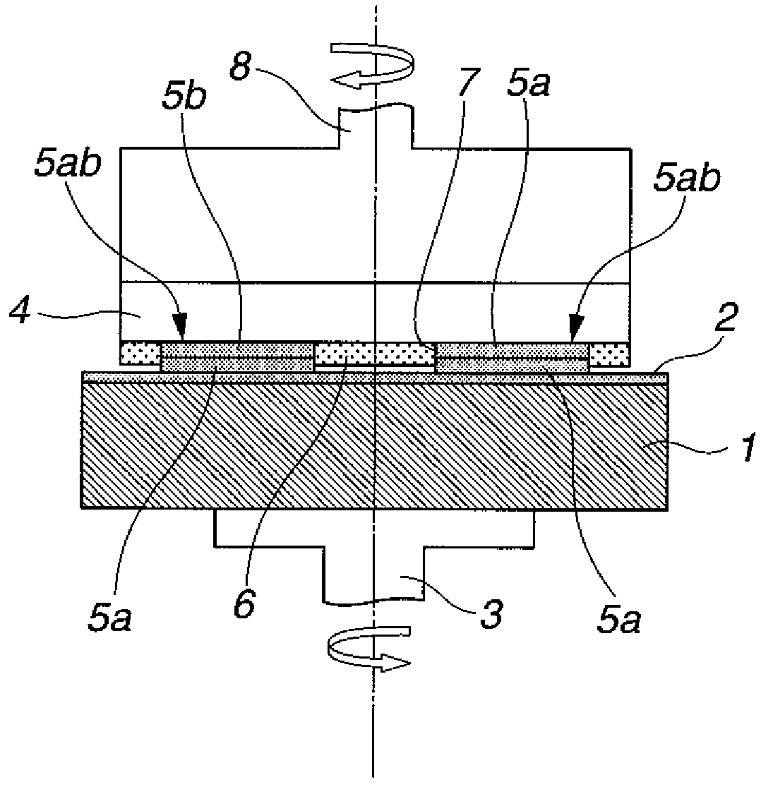
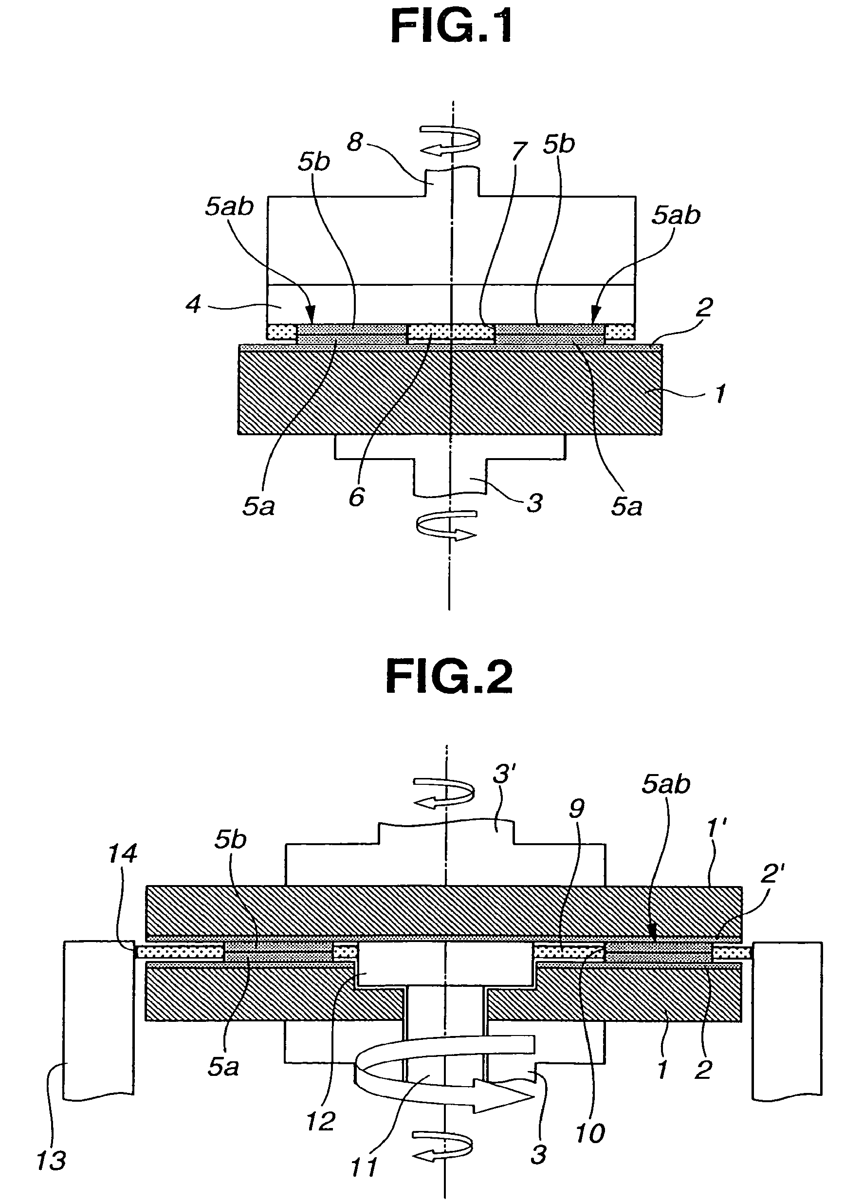
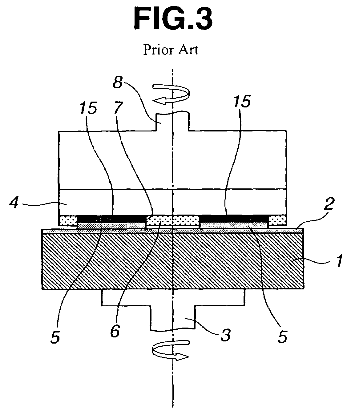
[0071]Then the substrate laminate 5ab was mirror poli...

example 2

[0075]This example relates to a lithium tantalate (LiTaO3) single crystal wafer having a diameter of 100 mm (4 inches). A single crystal ingot was grown by Czochralski method and sliced into wafers using a wire saw. The wafers as sliced were lapped on a double-side lapping machine with appropriate abrasives (loose abrasive grains) to a desired thickness and until the front and back surfaces reached the predetermined roughness state.

[0076]Then two wafers lapped as above (having front and back surfaces roughened) were laminated together, with their front surfaces (identical polarized surfaces) inside, using a wax Skyliquid TW-2511 (Nikka Seiko Co., Ltd.). Although a heat treatment is involved in the lamination step, this lamination ensures that the warpage of two wafers is offset because two wafers of the same material develop thermal expansion behavior in opposite directions. The laminate was ready for the subsequent lapping step.

[0077]Using a double-side lapping machine and adequate...

example 3

[0085]This example relates to a lithium tantalate (LiTaO3) single crystal wafer having a diameter of 100 mm (4 inches). A single crystal ingot was grown by Czochralski method and sliced into wafers using a wire saw. The wafers as sliced were lapped on a double-side lapping machine with appropriate abrasives (loose abrasive grains) to a desired thickness and until the front and back surfaces reached the predetermined roughness state.

[0086]Then two wafers lapped as above (having front and back surfaces roughened) were laminated together, with their back surfaces (identical polarized surfaces) inside, using a wax Skyliquid TW-2511 (Nikka Seiko Co., Ltd.). Although a heat treatment is involved in the lamination step, this lamination ensures that the warpage of two wafers is offset because two wafers of the same material develop thermal expansion behavior in opposite directions. The laminate was ready for the subsequent polishing step.

[0087]Then the substrate laminate 5ab was mirror poli...


PUM

PropertyMeasurementUnit
thicknessaaaaaaaaaa
thicknessaaaaaaaaaa
thicknessaaaaaaaaaa

Abstract

A wafer substrate is polished by disposing the wafer substrate between an abrasive cloth on a polishing platen and a plate, and relatively rotating the polishing platen and the plate for mirror polishing the surface of the wafer substrate with the abrasive cloth. A liquid is fed onto the plate side surface of the wafer substrate so that the wafer substrate is directly held to the plate by the adsorption force of the liquid, while performing the mirror polishing.

Description

CROSS-REFERENCE TO RELATED APPLICATION[0001]This non-provisional application claims priority under 35 U.S.C. §119(a) on Patent Application No. 2005-251026 filed in Japan on Aug. 31, 2005, the entire contents of which are hereby incorporated by reference.TECHNICAL FIELD[0002]This invention relates to a method for mirror polishing wafers, typically lithium tantalate single crystal wafers for use in surface acoustic wave (often abbreviated as SAW) filters.BACKGROUND ART[0003]In the mobile communications field including PHS and mobile phones, piezoelectric oxide single crystal wafers of lithium tantalate, lithium niobate, quartz, lithium tetraborate, langasite or the like are utilized as substrates of surface acoustic wave devices.[0004]The SAW device includes a piezoelectric oxide single crystal wafer as a substrate and interdigital electrodes deposited on one major surface of the substrate to provide a transducer. Since the device is constructed such that the transducer receives and e...

Claims


Application Information

Patent Timeline
Patent Type & Authority Patents(United States)
IPC IPC(8): B24B7/19B24B19/00B24B7/30B24B37/28B24B37/30
CPCB24B37/30B24B37/28H01L21/304
Inventor MURAI, TOSHINARISHIBANO, YUKIO
Owner SHIN ETSU CHEM CO LTD
Why Eureka
Try Eureka