Method and structure for fabricating bonded substrate structures using thermal processing to remove oxygen species

a technology of oxygen species and substrate structure, which is applied in the field of manufacturing substrates, can solve the problems of brittle materials, difficult to achieve the separation or cutting of materials that are difficult to achieve, and can not be used in the general direction of providing precision separation of substrates for the manufacture of fine tools and assemblies, etc., and achieves a wide range of applicability

Inactive Publication Date: 2009-10-06
SILICON GENERAL CORPORATION
View PDF83 Cites 24 Cited by
  • Summary
  • Abstract
  • Description
  • Claims
  • Application Information

AI Technical Summary

Benefits of technology

[0012]Numerous benefits are achieved over pre-existing techniques using the present invention. In particular, the present invention uses controlled energy and selected conditions to preferentially cleave and treat a thin film of material without a possibility of damage to such film from excessive energy release and / or thermal energy. This cleaving process selectively removes the thin film of material from the substrate while preventing a possibility of damage to the film or a remaining portion of the substrate. Additionally, the present method and structures allow for more efficient processing using a cleave layer provided in a substrate through the course of semiconductor processing, which may occur at higher temperatures, according to a specific embodiment. In a specific embodiment, the cleaved film, which is attached to a handle substrate, is subjected to a rapid thermal treatment process to firmly engage the cleaved film to the handle substrate without formation of imperfections within a vicinity of an interface region provided between the cleaved film and substrate. In a specific embodiment, the cleaved assembly can be subjected to a smoothing process as taught in U.S. Pat. No. 6,287,941 issued Sep. 11, 2001, and in the names of Kang, Sien G. and Malik, Igor J., commonly assigned (the '941 patent), or U.S. Pat. Nos. 6,884,696 and 6,962,858, each of which is incorporated by reference herein to prepare a clean and defect-free surface and followed by a single-wafer reactor or furnace anneal operation to effectuate the oxygen dissolution. In the case of the epi-smoothing in the '941 patent process, for example, additional cost benefits can be realized by combining the anneal as an additional treatment in-situ to the prior epi-smoothing process sequence. Depending upon the embodiment, one or more of these benefits may be achieved. These and other benefits may be described throughout the present specification and more particularly below.

Problems solved by technology

This technique, however, is often extremely “rough” and cannot generally be used for providing precision separations in the substrate for the manufacture of fine tools and assemblies.
Additionally, the saw operation often has difficulty separating or cutting extremely hard and or brittle materials, such as diamond or glass.
The saw operation also cannot be used effectively for the manufacture of microelectronic devices, including integrated circuit devices, and the like.
Making devices smaller is very challenging, as each process used in integrated circuit fabrication has a limit.
Additionally, as devices require faster and faster designs, process limitations exist with certain conventional processes and materials.
A conventional process often used to thin these device layers is often called “back grinding,” which is often cumbersome, prone to cause device failures, and can only thin the device layer to a certain thickness.
Although there have been significant improvements, such back grinding processes still have many limitations.

Method used


Image

  • Method and structure for fabricating bonded substrate structures using thermal processing to remove oxygen species
  • Method and structure for fabricating bonded substrate structures using thermal processing to remove oxygen species
  • Method and structure for fabricating bonded substrate structures using thermal processing to remove oxygen species

Examples


Embodiment Construction

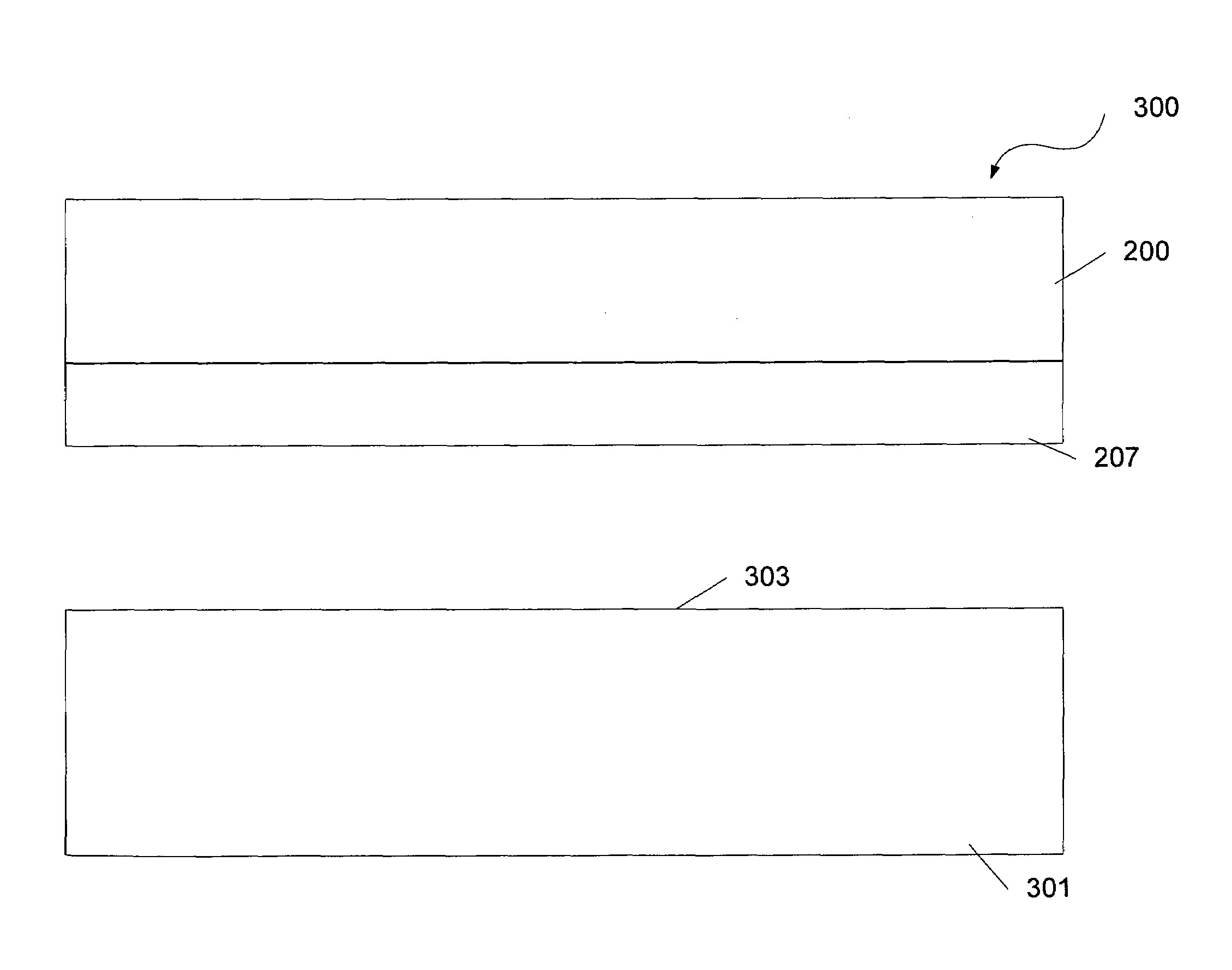
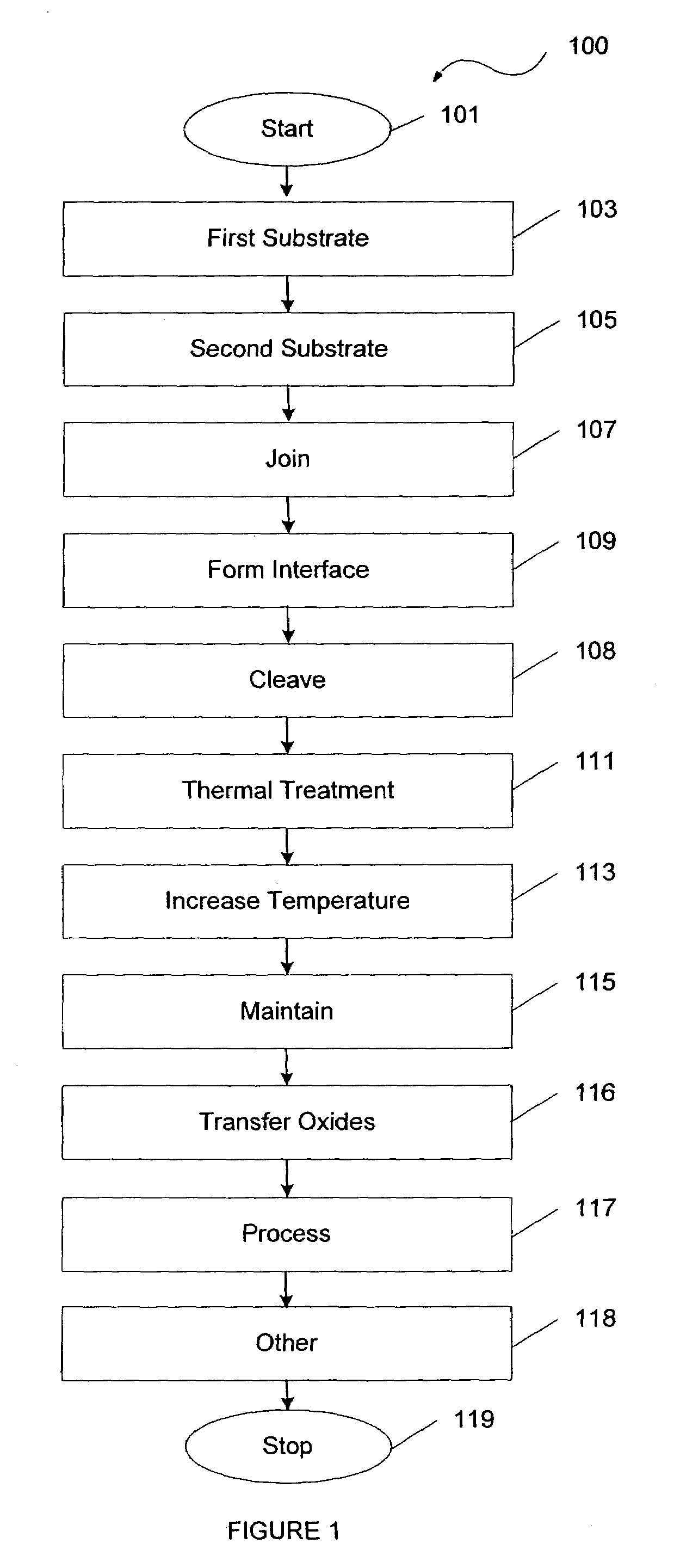
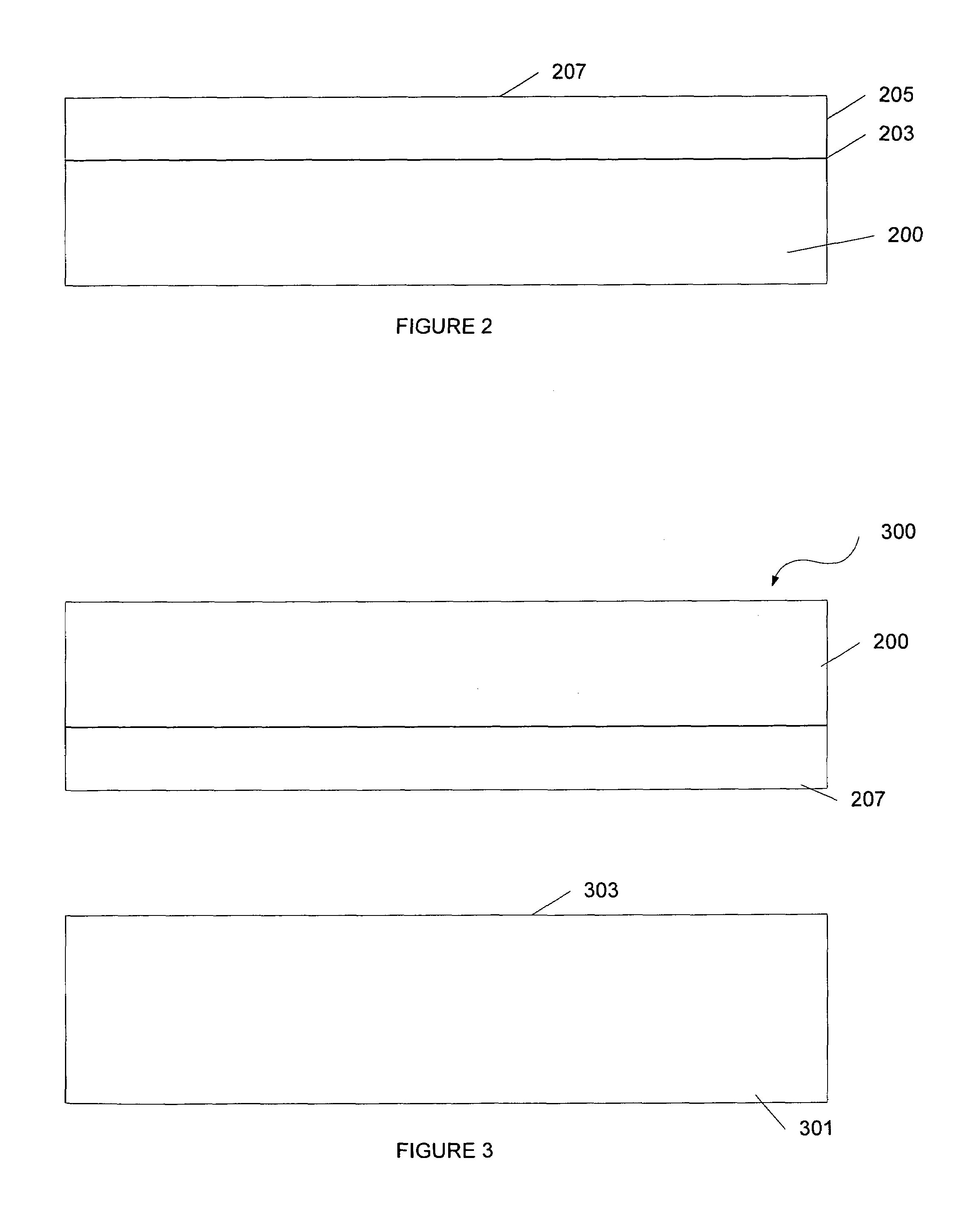
[0017]According to the present invention, techniques related to the manufacture of substrates are provided. More particularly, the invention provides a technique including a method and a structure for forming multi-layered substrate structures using bonding techniques for the fabrication of semiconductor integrated circuit devices. Such bonding techniques include use of thermal processing to establish bonded interfaces that are substantially free of imperfections, defects, and / or other undesirable features according to a specific embodiment. In a preferred embodiment, the thermal processing causes oxygen species to be transferred from an interface region between a bonded pair to be removed to an outer region. But it will be recognized that the invention has a wider range of applicability; it can also be applied to other types of substrates for three-dimensional packaging of integrated semiconductor devices, photonic devices, piezoelectronic devices, flat panel displays, microelectro...


PUM

PropertyMeasurementUnit
thicknessaaaaaaaaaa
thicknessaaaaaaaaaa
temperatureaaaaaaaaaa

Abstract

A method for fabricating bonded substrate structures, e.g., silicon on silicon. In a specific embodiment, the method includes providing a thickness of single crystal silicon material transferred from a first silicon substrate coupled to a second silicon substrate. In a specific embodiment, the second silicon substrate has a second surface region that is joined to a first surface region from the thickness of single crystal silicon material to form of an interface region having a first characteristic including a silicon oxide material between the thickness of single crystal silicon material and the second silicon substrate. The method includes subjecting the interface region to a thermal process to cause a change to the interface region from the first characteristic to a second characteristic. In a specific embodiment, the second characteristic is free from the silicon oxide material and is an epitaxially formed silicon material provided between the thickness of single crystal silicon material and the second silicon substrate. The method includes maintaining the interface region free of multiple voids during the thermal process to form the epitaxially formed silicon material to electrically couple the thickness of single crystal silicon material to the second silicon substrate.

Description

BACKGROUND OF THE INVENTION[0001]The present invention relates to the manufacture of substrates. More particularly, the invention provides a technique including a method and a structure for forming multi-layered substrate structures using bonding techniques for the fabrication of semiconductor integrated circuit devices. Such bonding techniques include use of thermal processing to establish bonded interfaces that are substantially free of imperfections, defects, and / or other undesirable features according to a specific embodiment. In a preferred embodiment, the thermal processing causes oxygen species to be transferred from an interface region between a bonded pair to be removed to an outer region. But it will be recognized that the invention has a wider range of applicability; it can also be applied to other types of substrates for three-dimensional packaging of integrated semiconductor devices, photonic devices, piezoelectronic devices, flat panel displays, microelectromechanical ...

Claims


Application Information

Patent Timeline
Patent Type & Authority Patents(United States)
IPC IPC(8): H01L21/30H01L21/46
CPCH01L21/76254H01L21/30G06Q50/04
Inventor HENLEY, FRANCOIS J.SULLIVAN, JAMES ANDREWKANG, SIEN GIOKONG, PHILIP JAMESKIRK, HARRY ROBERTJACY, DAVIDMALIK, IGOR
Owner SILICON GENERAL CORPORATION
Why Eureka
Try Eureka