
Controlled process and resulting device

a technology of controlled process and resulting device, which is applied in the direction of semiconductor devices, chemistry apparatus and processes, electrical equipment, etc., can solve the problems of brittle materials, difficult to achieve the separation or cutting of materials that are extremely hard and/or brittle, and cannot generally be used to provide precision separation of substrates for the manufacture of fine tools and assemblies

Inactive Publication Date: 2014-09-16
SILICON GENERAL CORPORATION
View PDF11 Cites 2 Cited by
  • Summary
  • Abstract
  • Description
  • Claims
  • Application Information

AI Technical Summary

Benefits of technology

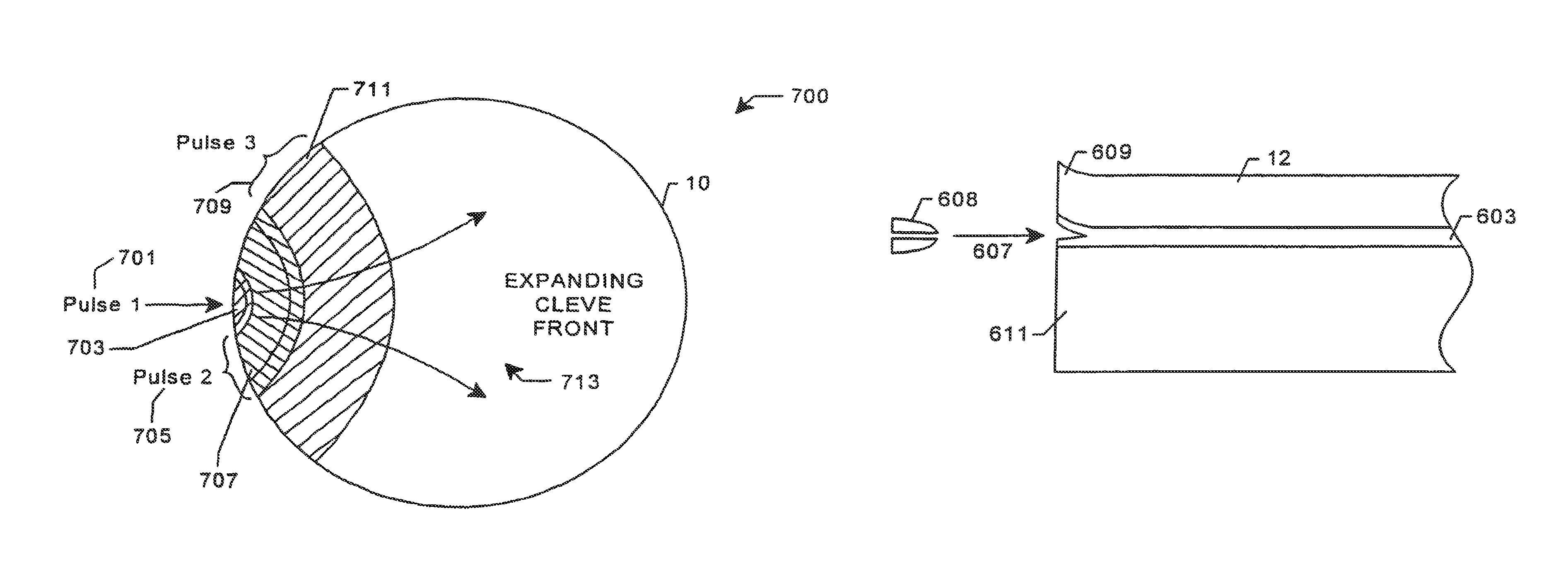
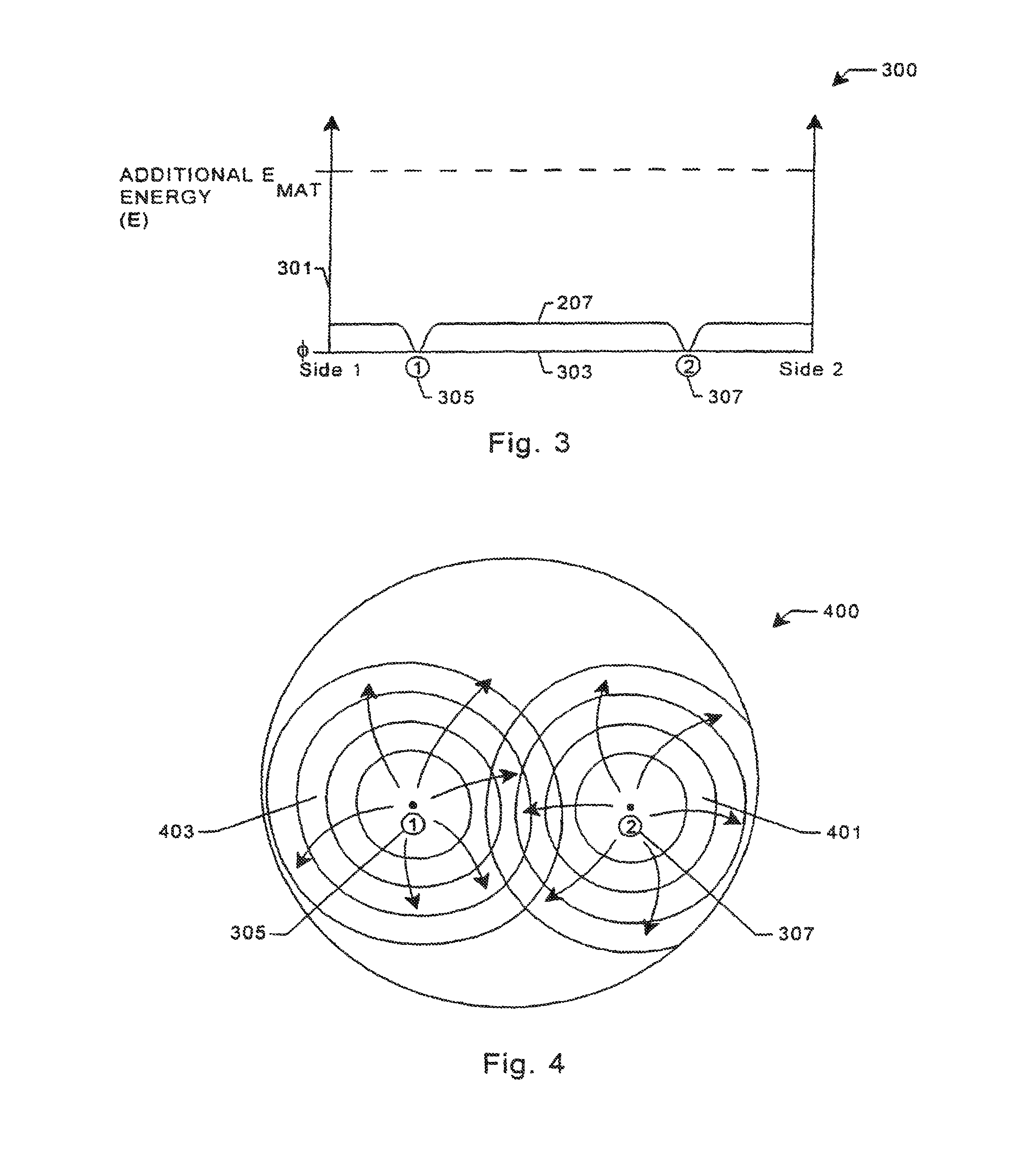
The present invention provides an improved technique for removing a thin film of material from a substrate using a controlled cleaving action. This technique uses controlled energy and selected conditions to initiate a cleaving process and allow it to propagate through the substrate to remove a thin film of material while minimizing damage to the substrate. The technique also reduces temperature excursions and damage caused by higher than necessary stress or pressure effects and nucleation sites as compared to pre-existing techniques. The remaining substrate portion can be re-used repeatedly for other applications.

Problems solved by technology

This technique, however, is often extremely “rough” and cannot generally be used for providing precision separations in the substrate for the manufacture of fine tools and assemblies.
Additionally, the saw operation often has difficulty separating or cutting extremely hard and / or brittle materials, such as diamond or glass.
Although the techniques described above are satisfactory, for the most part, as applied to cutting diamonds or household glass, they have severe limitations in the fabrication of small complex structures or precision workpieces.
For instance, the above techniques are often “rough” and cannot be used with great precision in fabrication of small and delicate machine tools, electronic devices, or the like.
Additionally, the above techniques may be useful for separating one large plane of glass from another, but are often ineffective for splitting off, shaving, or stripping a thin film of material from a larger substrate.
Furthermore, the above techniques may often cause more than one cleave front, which join along slightly different planes, which is highly undesirable for precision cutting applications.

Method used


Image

  • Controlled process and resulting device
  • Controlled process and resulting device
  • Controlled process and resulting device

Examples


Embodiment Construction

[0022]The present invention provides a technique for removing a thin film of material from a substrate while preventing a possibility of damage to the thin material film and / or a remaining portion of the substrate. The thin film of material is attached to or can be attached to a target substrate to form, for example, a silicon-on-insulator wafer. The thin film of material can also be used for a variety of other applications. The invention will be better understood by reference to the Figs. and the descriptions below.

[0023]1. Controlled Cleaving Techniques

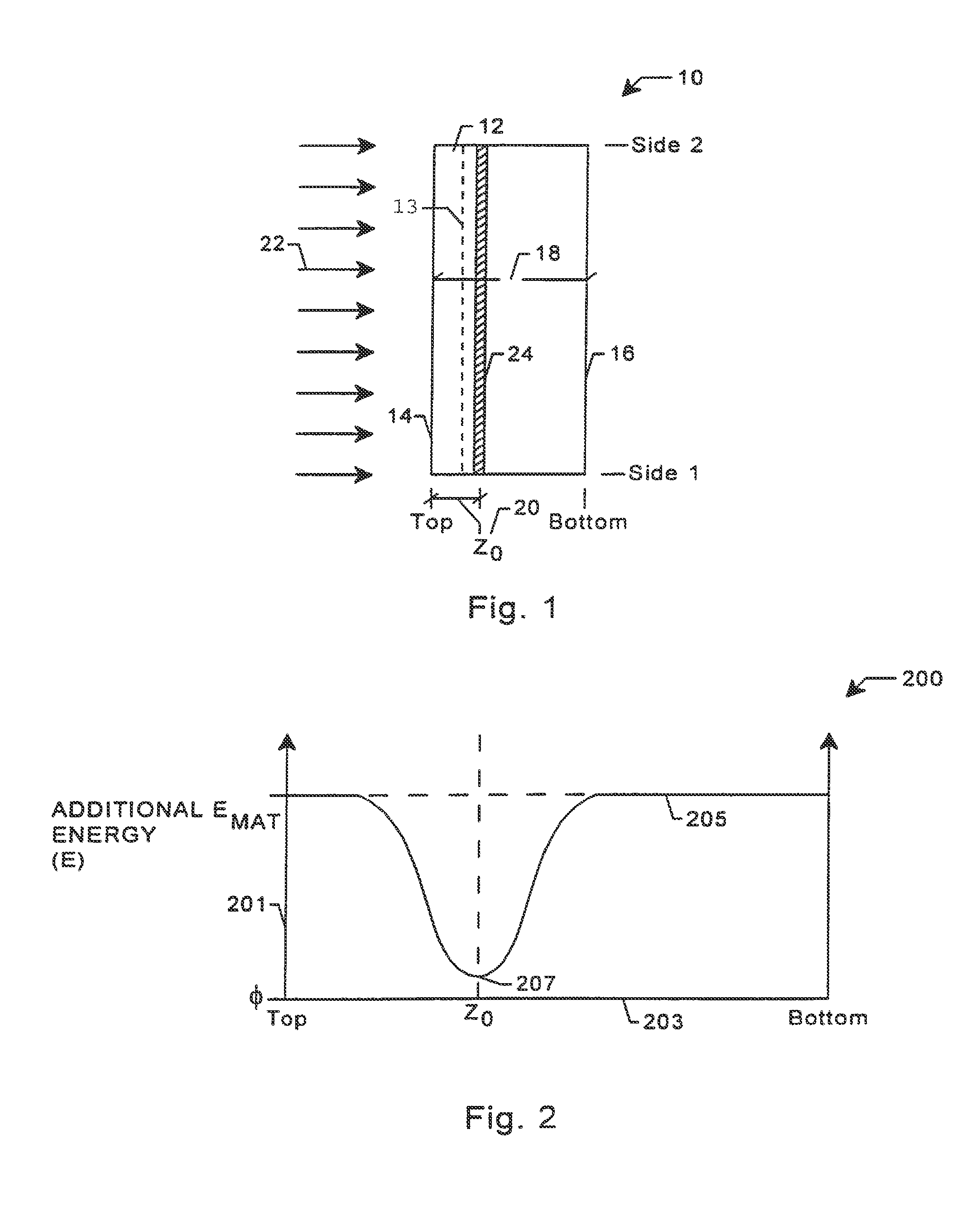
[0024]FIG. 1 is a simplified cross-sectional view diagram of a substrate 10 according to the present invention. The diagram is merely an illustration and should not limit the scope of the claims herein. Although the description below is in terms of a silicon wafer, other substrates may also be used. For example, the substrate can be almost any monocrystalline, polycrystalline, or even amorphous type substrate. Additionally, the subs...


PUM


Abstract

A method for forming a multi-material thin film includes providing a multi-material donor substrate comprising single crystal silicon and an overlying film comprising GaN. Energetic particles are introduced through a surface of the multi-material donor substrate to a selected depth within the single crystal silicon. The method includes providing energy to a selected region of the donor substrate to initiate a controlled cleaving action in the donor substrate. Then, a cleaving action is made using a propagating cleave front to free a multi-material film from a remaining portion of the donor substrate, the multi-material film comprising single crystal silicon and the overlying film.

Description

CROSS-REFERENCES TO RELATED APPLICATIONS[0001]This application is a continuation-in-part of U.S. application Ser. No. 13 / 207,304 filed on Aug. 10, 2011, which is a continuation of U.S. application Ser. No. 12 / 789,361 filed on May 27, 2010, which is a continuation of U.S. application Ser. No. 12 / 218,149 filed on Jul. 10, 2008, which is a continuation of U.S. application Ser. No. 11 / 627,920 filed on Jan. 26, 2007, which is a continuation of U.S. application Ser. No. 11 / 281,042 filed on Nov. 16, 2005, which is a continuation of U.S. application Ser. No. 10 / 644,644 filed on Aug. 19, 2003, which is a continuation of U.S. application Ser. No. 09 / 483,393 filed Jan. 13, 2000, which is a continuation of U.S. application Ser. No. 09 / 026,034 filed Feb. 19, 1998, which claims priority from the U.S. provisional patent application entitled A CONTROLLED CLEAVAGE PROCESS AND RESULTING DEVICE, filed May 12, 1997 and assigned Application No. 60 / 046,276. The disclosure of all of the above applications...

Claims


Application Information

Patent Timeline
Patent Type & Authority Patents(United States)
IPC IPC(8): H01L21/46H01L21/425H01L21/18H01L21/20H01L21/223H01L21/265H01L21/268H01L21/304H01L21/762H01L21/78
CPCH01L21/268H01L21/187H01L21/2236H01L21/7624H01L21/2007H01L21/76254H01L21/304H01L21/7813Y10S438/977H01L21/26506Y10S438/974Y10S117/915Y10S156/93H01L21/265H01L21/2658H01L21/26593
Inventor HENLEY, FRANCOIS J.CHEUNG, NATHAN
Owner SILICON GENERAL CORPORATION
Learn More