Offset etched corner leads for semiconductor package

a technology of offset etched corners and semiconductors, applied in semiconductor devices, semiconductor/solid-state device details, electrical apparatus, etc., to achieve the effects of superior board level reliability, increased die pad size, and increased length

Active Publication Date: 2009-10-06
AMKOR TECH SINGAPORE HLDG PTE LTD
View PDF325 Cites 6 Cited by
  • Summary
  • Abstract
  • Description
  • Claims
  • Application Information

AI Technical Summary

Benefits of technology

[0011]In an alternative embodiment of the present invention, the leads of the leadframe are identically configured, with each such lead including a recessed lead shelf formed within the top lead surface adjacent the peripheral edge of the die pad. In the alternative embodiment, each of the leads further includes a pair of ear portions extending laterally from respective sides of each of the leads in opposed relation to each other. The ear portions each have a top ear surface which extends in generally co-planar relation to the top lead surface and a bottom ear surface which is recessed relative to the bottom lead surface. The inclusion of the recessed lead shelf within each of the leads of this alternative embodiment allows for an increase in the size of the die pad of the leadframe.
[0012]In each embodiment of the present invention, the bottom lead surfaces define lands which are of increased length to provide superior board level reliability. In addition to the increased length lands defined by the leads of the leadframes constructed in accordance with the present invention, the structural attributes of such leadframes also provide any semiconductor package fabricated to include the same with a maximum lead count in addition to the optimum board level reliability attributable to the increased land lengths.

Problems solved by technology

An overall limitation of the design of the above-described semiconductor package pertains to the electrical connections and configurations utilized to satisfy the required electrical inputs and outputs to and from the input / output terminals of the semiconductor die.

Method used


Image

  • Offset etched corner leads for semiconductor package
  • Offset etched corner leads for semiconductor package
  • Offset etched corner leads for semiconductor package

Examples


Embodiment Construction

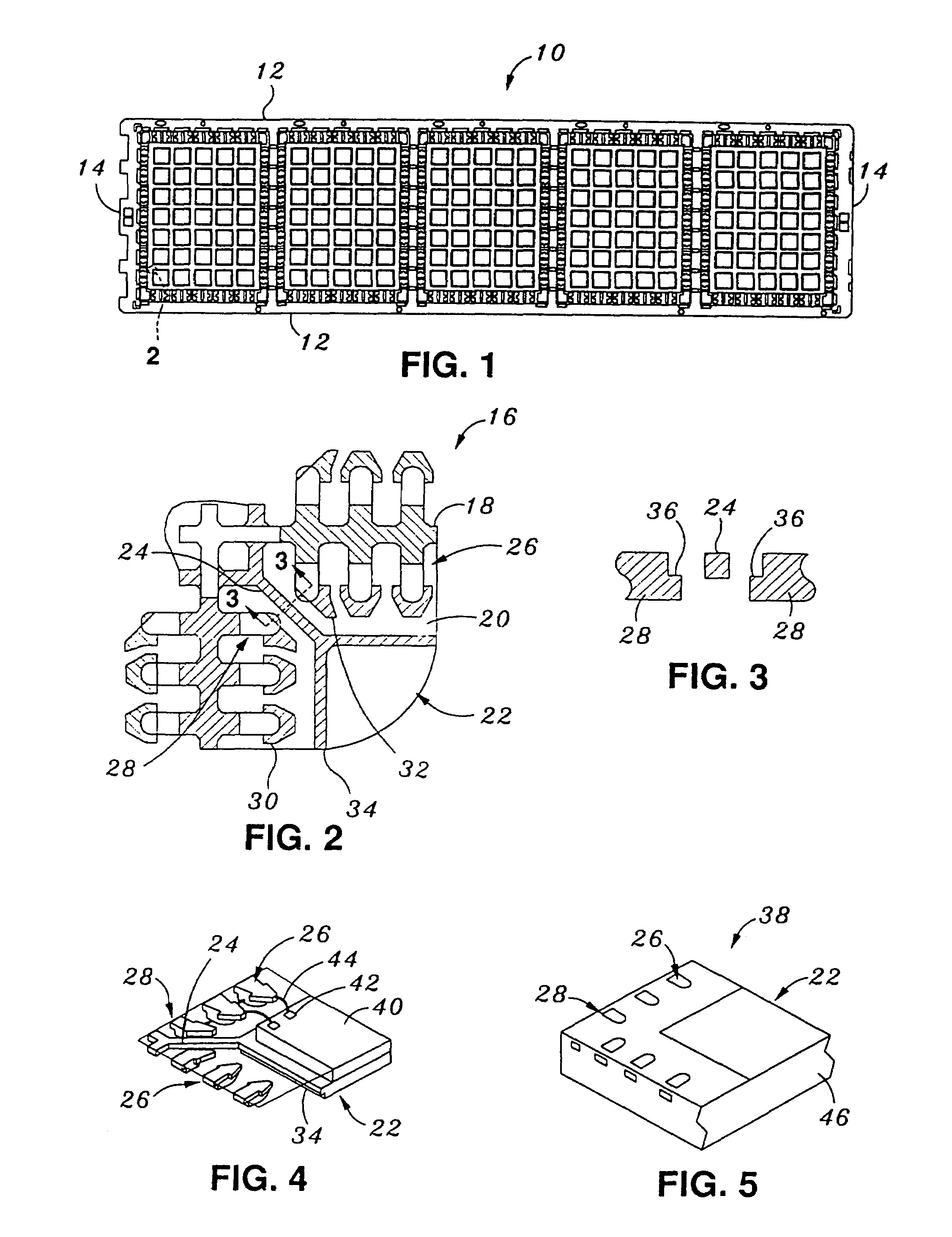
[0026]Referring now to the drawings, FIG. 1 depicts a leadframe strip 10 constructed in accordance with the present invention. The leadframe strip 10 has a generally rectangular configuration, defining an opposed pair of longitudinal peripheral edge segments 12 and an opposed pair of lateral peripheral edge segments 14. The strip 10 defines a multiplicity of identically configured leadframes 16. Those of ordinary skill in the art will recognize that the number and arrangement of the leadframes 16 shown in FIG. 1 are exemplary only, and that the strip 10 may be fabricated to define any number of leadframes 16 arranged in a multiplicity of different configurations or arrays without departing from the spirit and scope of the present invention.

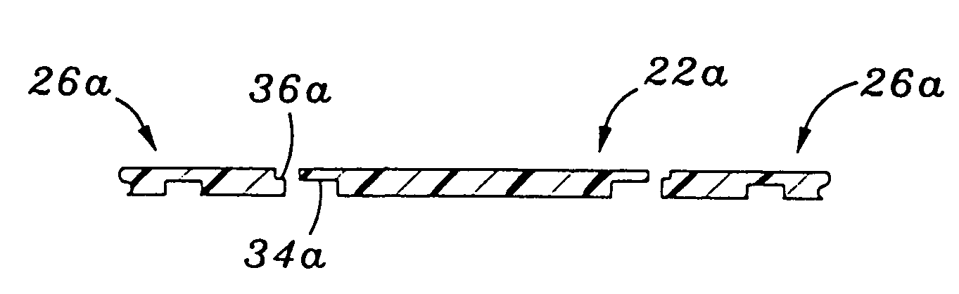
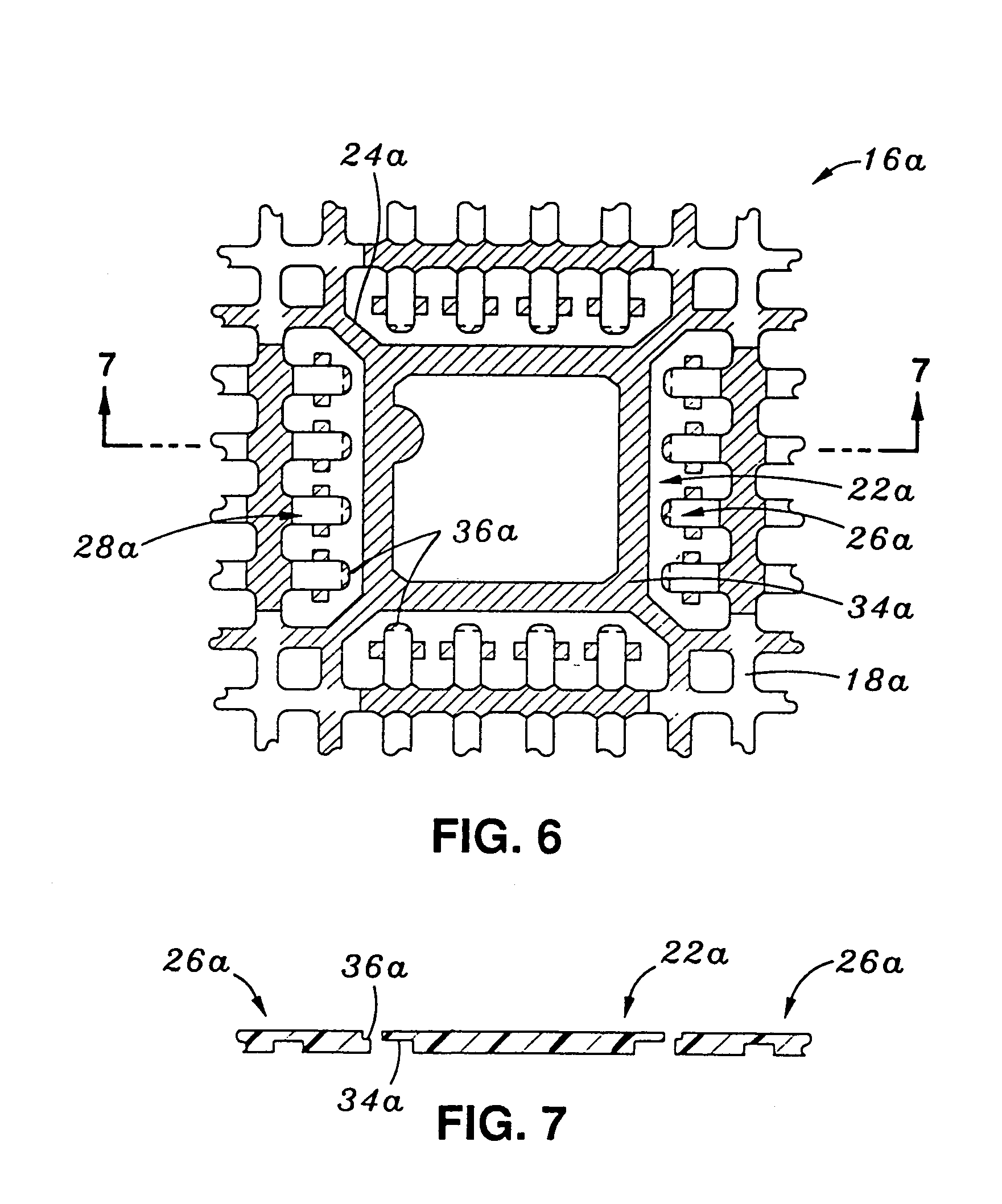
[0027]Referring now to FIG. 2, each leadframe 16 comprises a generally square outer frame portion 18 which defines a centrally positioned, generally square opening 20. Disposed within the opening 20 is a die pad 22 of the leadframe 16. The die pad...


PUM


Abstract

A semiconductor package comprising a leadframe. The leadframe itself comprises an outer frame portion which defines a central opening. Disposed within the central opening is a die pad which defines opposed, generally planar top and bottom die pad surfaces and a peripheral edge. Connected to and extending between the outer frame portion and the peripheral edge of the die pad is at least one tie bar of the leadframe. The leadframe also includes a plurality of leads which are connected to the outer frame portion and extend into the opening at least partially about the die pad in spaced relation to the peripheral edge thereof. Each of the leads includes opposed, generally planar top and bottom lead surfaces, with at least two of the leads comprising corner leads which extend along opposed sides of the tie bar. Each of the corner leads further defines an angularly offset distal portion which extends along and in spaced relation to the tie bar.

Description

CROSS-REFERENCE TO RELATED APPLICATIONS[0001]The present application is a divisional of U.S. application Ser. No. 10 / 358,621 entitled OFFSET ETCHED CORNER LEADS FOR SEMICONDUCTOR PACKAGE filed Feb. 5, 2003 now U.S. Pat. No. 6,847,099.STATEMENT RE: FEDERALLY SPONSORED RESEARCH / DEVELOPMENT[0002](Not Applicable)BACKGROUND OF THE INVENTION[0003]1. Field of the Invention[0004]The present invention relates generally to semiconductor packages and, more particularly, to a semiconductor package which includes offset etched corner leads to allow etching beyond a minimum capable distance between the die pad tie bars and adjacent lands, or leads which are etched in a manner allowing for an increase in the size of the die pad.[0005]2. Description of the Related Art[0006]The current trend in the electronics industry is to provide electronic devices which are multi-functional, compact, and capable of achieving high performance levels. In view of this trend, a requirement has arisen that the semico...

Claims


Application Information

Patent Timeline
Patent Type & Authority Patents(United States)
IPC IPC(8): H01L23/495H01L21/48H01L23/31
CPCH01L21/4821H01L23/3107H01L23/49548H01L24/48H01L2224/48247H01L2224/48091H01L2924/00014H01L2224/05554H01L2224/97H01L2924/18301H01L2224/45099H01L2224/45015H01L2924/207
Inventor BANCOD, LUDOVICODELA CRUZ, GREGORIO G.CANOY, FIDELYN R.ALABIN, LEOCADIO M.
Owner AMKOR TECH SINGAPORE HLDG PTE LTD
Why Eureka
Try Eureka