Supercharge Your Innovation With Domain-Expert AI Agents!

Semiconductor memory device and method of testing the same

a technology of memory devices and semiconductors, applied in the direction of separation processes, instruments, transportation and packaging, etc., can solve the problems of high cost and relative long time required for memory tes

Active Publication Date: 2009-10-20
SAMSUNG ELECTRONICS CO LTD
View PDF12 Cites 7 Cited by
  • Summary
  • Abstract
  • Description
  • Claims
  • Application Information

AI Technical Summary

Benefits of technology

The patent text describes a semiconductor memory device with built-in self-test (BIST) circuits. These circuits generate test pattern data and compare it to received test pattern data to verify the proper operation of the device. The technical effect of this invention is to improve the efficiency and accuracy of testing semiconductor memory devices during production.

Problems solved by technology

When performing the memory test using the external memory test device having an operating frequency lower than that of the semiconductor memory device, a relatively long time is required for the memory test.
When performing the memory test using the external memory test device having the operating frequency identical with that of the semiconductor memory device, a high cost is incurred.

Method used


Image

  • Semiconductor memory device and method of testing the same
  • Semiconductor memory device and method of testing the same
  • Semiconductor memory device and method of testing the same

Examples


Embodiment Construction

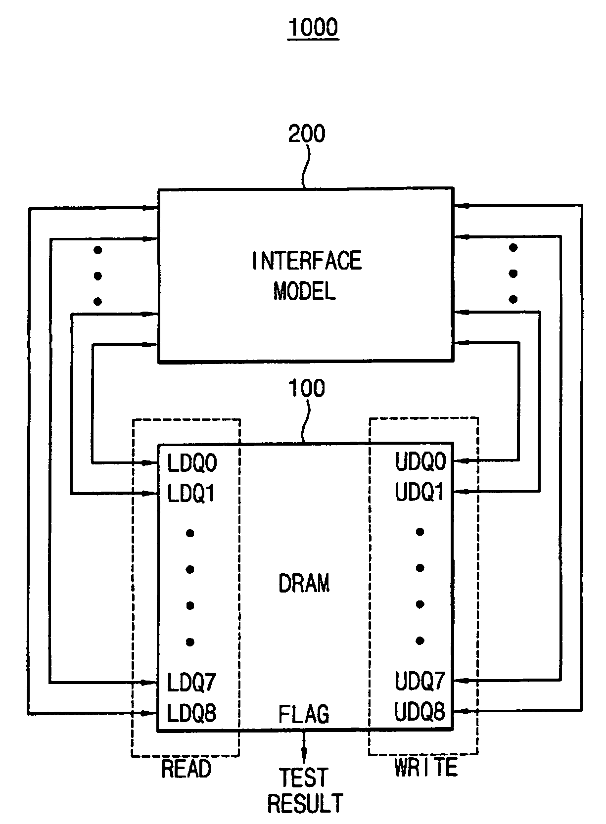
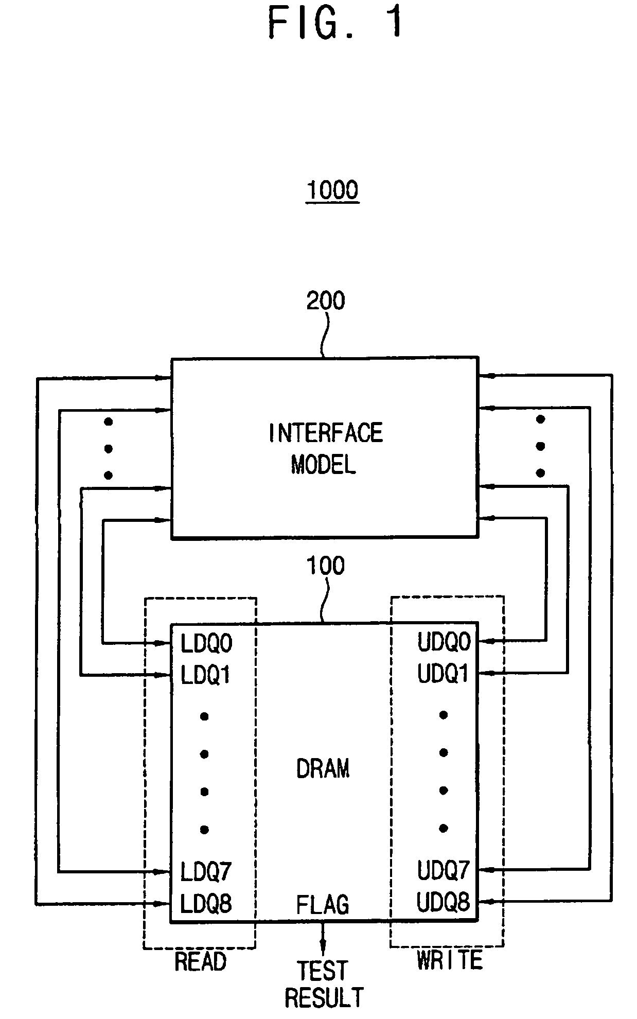
[0017]Embodiments are disclosed herein. However, specific structural and functional details disclosed herein are merely representative for purposes of describing example embodiments. This invention may, however, be embodied in many alternate forms and should not be construed as limited to the embodiments set forth herein.

[0018]Accordingly, while other embodiments are susceptible to various modifications and alternative forms, specific embodiments are shown by way of example in the drawings and will be described in detail. It should be understood, however, that there is no intent to limit the invention to the particular forms disclosed, but, on the contrary, the invention is to cover all modifications, equivalents, and alternatives falling within the spirit and scope of the invention. Like numbers refer to like elements throughout the description of the figures.

[0019]It will be understood that, although the terms first, second, etc. may be used to describe various elements, these ele...


PUM

PropertyMeasurementUnit
operating frequencyaaaaaaaaaa
phase erroraaaaaaaaaa
operating speedaaaaaaaaaa

Abstract

A semiconductor memory device includes at least one first built in self test (BIST) circuit configured to generate test pattern data, and at least one second BIST circuit configured to receive the test pattern data as received test pattern data and compare the received test pattern data to the test pattern data.

Description

CLAIM FOR PRIORITY[0001]This application claims priority to Korean Patent Application No. 10-2005-0011525 filed on Feb. 11, 2005 in the Korean Intellectual Property Office, the entire contents of which are herein incorporated by reference.BACKGROUND OF THE INVENTION[0002]1. Field of the Invention[0003]This disclosure relates to a method of testing of a semiconductor memory device, and more particularly to a method of testing a semiconductor memory device using a built-in self-test (BIST) circuit and a semiconductor memory device having a BIST circuit.[0004]2. Description of the Related Art[0005]In a conventional method of testing a memory device, data read from a memory array are output to a data output buffer, the output data are provided to an external memory test device through a data output pad, and then, the external memory test device performs a memory test operation using the output data.[0006]When performing the memory test using the external memory test device having an ope...

Claims


Application Information

Patent Timeline
Patent Type & Authority Patents(United States)
IPC IPC(8): G11C29/00G01R31/28G06F11/00
CPCG11C29/1201G11C29/36G11C11/401G11C2029/3602G11C2029/0405B01D47/063B01D47/12B01D53/78B01D46/4272B01D46/44B01D46/0031B01D2259/455B01D46/66B01D50/60
Inventor JUNG, DAE-HEEPARK, CHUL-WOOSEO, SEUNG-YOUNG
Owner SAMSUNG ELECTRONICS CO LTD
Features
  • R&D
  • Intellectual Property
  • Life Sciences
  • Materials
  • Tech Scout
  • Unparalleled Data Quality
  • Higher Quality Content
  • 60% Fewer Hallucinations
Learn More