Spin transistor using stray magnetic field

a technology of spin transistor and magnetic field, which is applied in the field of spin transistor, can solve the problems of difficult to obtain clear signals from the spin transistor, low injection efficiency of spin information, etc., and achieve the effect of high spin transmission

Inactive Publication Date: 2009-10-27
KOREA INST OF SCI & TECH
View PDF14 Cites 21 Cited by
  • Summary
  • Abstract
  • Description
  • Claims
  • Application Information

AI Technical Summary

Benefits of technology

[0008]The present invention has been made to solve the foregoing problems of the prior art and therefore an aspect of the present invention is to provide a spin transistor which can transmit spin information to charges without passing through a junction surface between a semiconductor and a ferromagnetic material, and has very high spin transmission effect.

Problems solved by technology

However, the semiconductor and the ferromagnetic material, including metal, are significantly different from each other in electric conductivity.
Thus, the injection efficiency of the spin information is very low.
That is, the information may be lost when passing through a junction surface therebetween and thus a clear signal is difficult to obtain from the spin transistor.

Method used


Image

  • Spin transistor using stray magnetic field
  • Spin transistor using stray magnetic field
  • Spin transistor using stray magnetic field

Examples


Embodiment Construction

[0030]Exemplary embodiments of the present invention will now be described in detail with reference to the accompanying drawings.

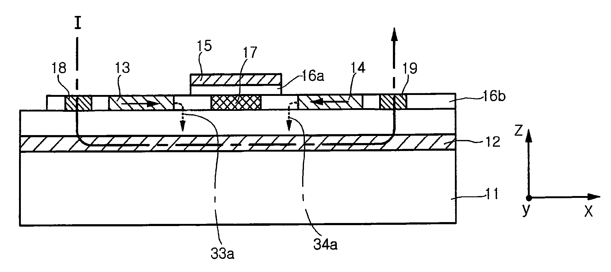
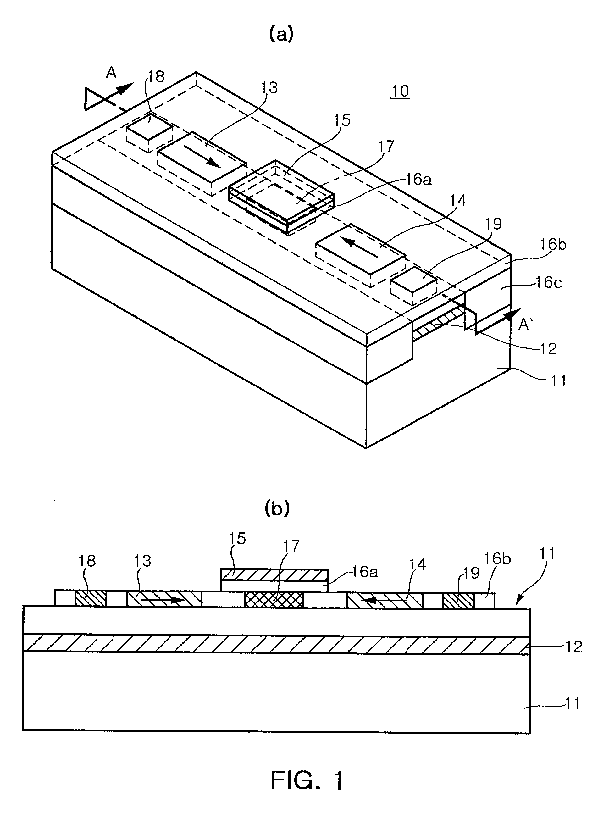
[0031]FIGS. 1(a) and 1(b) are, respectively, a perspective view and a cross-sectional view of a spin transistor according to an exemplary embodiment of the present invention.

[0032]Referring to FIGS. 1(a) and 1(b), the spin transistor 10 according to the present embodiment includes a semiconductor substrate 11 having a channel layer 12 formed therein, and first and second electrodes 18 and 19, a source 13, a gate 15 and a drain 14, all of which are formed on the semiconductor substrate 11.

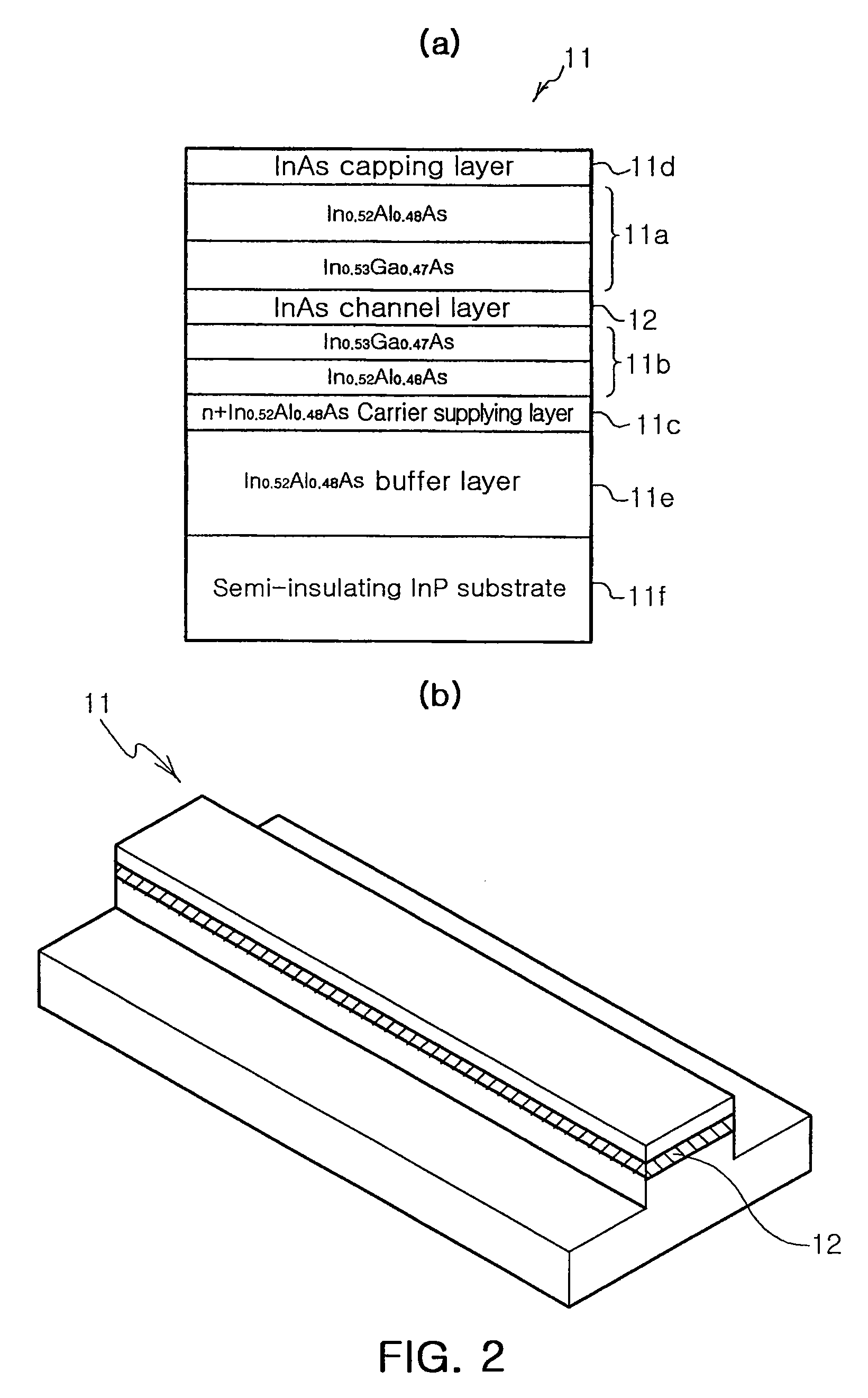
[0033]The semiconductor substrate 11 has a ridge structure in which the parts of the both sides of the channel layer 12 are cut out. The width of the channel layer 12 is defined by the ridge structure. The substrate having the ridge structure may be formed using lithography and ion milling.

[0034]The width of the channel layer 12 is defined by the length of a protruded regi...


PUM


Abstract

Disclosed herein is a spin transistor including: a semiconductor substrate having a channel layer formed therein; first and second electrodes which are formed to be spaced apart from each other on the substrate at a predetermined distance along a longitudinal direction of the channel layer; a source and drain which include magnetized ferromagnetic materials and are formed to be spaced apart form each other between the first electrode and the second electrode at a predetermined distance along the longitudinal direction of the channel layer; and a gate which is formed on the substrate between the source and the drain, and adjusts spin orientations of electrons passing through the channel layer, wherein the electrons passing through the channel layer are spin-aligned at a lower side of the source by a stray magnetic field of the source and spin-filtered at a lower side of the drain by a stray field of the drain.

Description

CLAIM PRIORITY[0001]This application claims the benefit of Korean Patent Application No. 2007-000888 filed on Jan. 4, 2007, in the Korean Intellectual Property Office, the disclosure of which is incorporated herein by reference.BACKGROUND OF THE INVENTION[0002]1. Field of the Invention[0003]The present invention relates to a spin transistor, and more particularly to a spin transistor which receives spin information through a source using a strong stray magnetic field generated by a ferromagnetic material, adjusts a spin orientation by the control of a gate, and selectively outputs electrons in a desired spin orientation through a drain.[0004]2. Description of the Related Art[0005]Today, a representative element of integrated circuit (IC) technology is based on a metal oxide semiconductor field effect transistor (MOSFET). A memory element such as DRAM or flash memory, an application specific integrated circuit (ASIC), a microprocessor, or a logic circuit includes a MOSFET for ON / OFF ...

Claims


Application Information

Patent Timeline
Patent Type & Authority Patents(United States)
IPC IPC(8): H01L29/72
CPCG11C11/16H01L29/0843H01L29/66984Y10S977/933Y10S257/902
Inventor KOO, HYUN CHEOLEOM, JONG HWAHAN, SUK HEECHANG, JOON YEONKIM, HYUNG JUN
Owner KOREA INST OF SCI & TECH
Why Eureka
Try Eureka