Power on detection circuit
a detection circuit and power supply technology, applied in the direction of pulse automatic control, pulse technique, electronic switching, etc., can solve the problems of increasing current consumption, increasing current consumption, and increasing current consumption, and causing the detection accuracy to be questionabl
- Summary
- Abstract
- Description
- Claims
- Application Information
AI Technical Summary
Benefits of technology
Problems solved by technology
Method used
Image

Examples
first embodiment
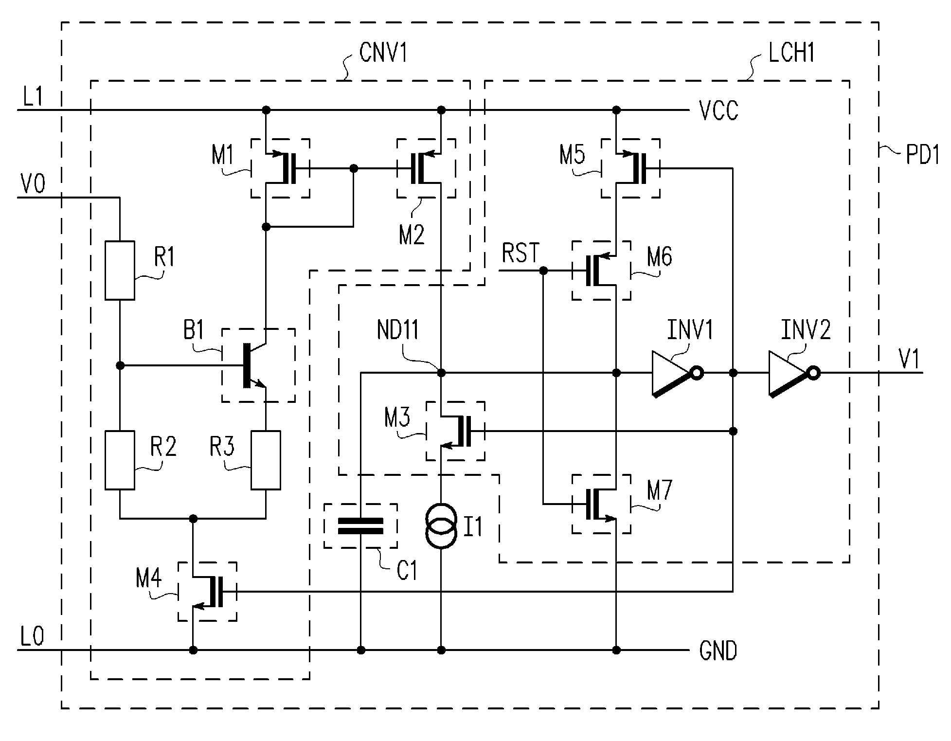
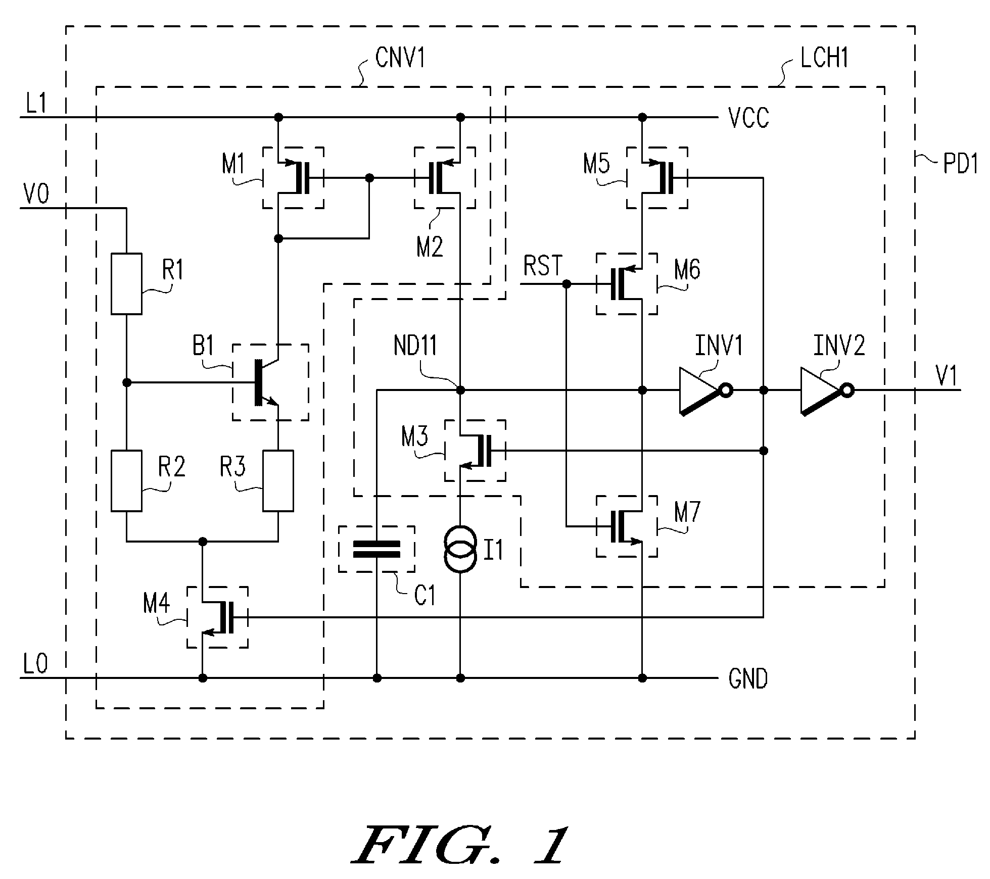
[0032]An output voltage V1 at the output terminal of the inverter INV2 is output as a power on detection signal of the power on detection circuit PD1. In the first embodiment, the transistors M3, M5, M6, and M7 and the inverters INV1 and INV2 form the latch circuit LCH1.
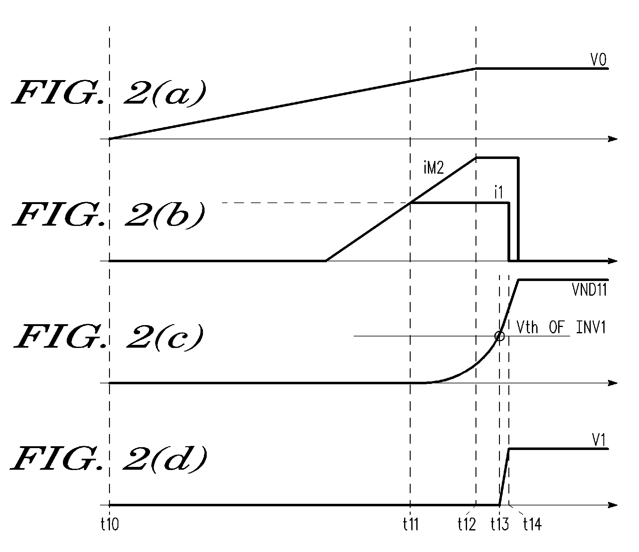
[0033]The operation of the power on detection circuit PD1 will now be described with reference to FIGS. 2(a) to 2(d). FIG. 2(a) shows the input voltage V0, FIG. 2(b) shows the currents i1 and iM2, FIG. 2(c) shows the voltage VND11 at the connection node ND11, and FIG. 2(d) shows the time dependency of the output voltage V1.
[0034]At time t10, the input voltage V0 increases from a common potential (0 V). In this case, the input voltage V0 is divided by the resistors R1 and R2, and the divided voltage is supplied to the base terminal of the transistor B1. The input voltage V0 must reach a predetermined voltage and activate the transistor B1 for current to flow to the transistor M1.
[0035]When the transistor B1 is activat...
second embodiment
[0051]In the second embodiment, a power on detection circuit PD2 includes a voltage conversion circuit CNV2, a latch circuit LCH2, and the current comparison circuit CMP2. The voltage conversion circuit CNV2 serves as a converting means for converting voltage to current. The latch circuit LCH2 serves as a latching means for holding a power on detection signal. The current comparison circuit CMP2 serves as a current comparator.
[0052]The voltage conversion circuit CNV2 has a structure that is in correspondence with the voltage conversion circuit CNV1 of the first embodiment. However, the voltage conversion circuit CNV2 of the second embodiment does not include the transistor M4 of the voltage conversion circuit CNV1.
[0053]In the same manner as in the first embodiment, the drain terminal of the transistor M2 in the voltage conversion circuit CNV2 is connected to the drain terminal of the transistor M3 and the capacitor C1 via a connection node ND21 (corresponding to the connection node...
third embodiment
[0071]In the third embodiment, the output terminal of the inverter INV1 is connected to the gate terminals of the transistors M3, M4, and M12.
[0072]In addition to the advantages of the second embodiment, the power on detection circuit PD3 of the third embodiment has the advantages described below.
[0073]In the third embodiment, when the input voltage causes the power to go on, the low level output of the inverter INV1 is provided to the gate terminal of the transistor M4. This deactivates the transistor M4 and stops the flow of current iM1 in the transistor M1. As a result, power consumption is reduced.
[0074]A fourth embodiment of the present invention will now be discussed with reference to FIGS. 6 and 7. The fourth embodiment differs from the third embodiment only in that a voltage conversion circuit CNV5 is formed by simplifying the voltage conversion circuit CNV3 of the third embodiment. The other parts are the same as the third embodiment and thus will not be described in detail...
PUM
 Abstract
Description
Claims
Application Information
 - R&D
- Intellectual Property
- Life Sciences
- Materials
- Tech Scout
- Unparalleled Data Quality
- Higher Quality Content
- 60% Fewer Hallucinations
Browse by: Latest US Patents, China's latest patents, Technical Efficacy Thesaurus, Application Domain, Technology Topic, Popular Technical Reports.
© 2025 PatSnap. All rights reserved.Legal|Privacy policy|Modern Slavery Act Transparency Statement|Sitemap|About US| Contact US: help@patsnap.com