CMOS image sensor with noise cancellation

a cmos image sensor and noise cancellation technology, applied in the field of semiconductor image sensors, can solve the problems of inability to develop a cmos sensor with the same snr and pixel pitch requirements, inability to meet the requirements of pixel pitch, and relatively inefficient approach, and achieve the effect of avoiding errors associated with storing and retrieving signals

Inactive Publication Date: 2009-11-03
CANDELA MICROSYST
View PDF4 Cites 139 Cited by
  • Summary
  • Abstract
  • Description
  • Claims
  • Application Information

AI Technical Summary

Problems solved by technology

To date there has not been developed a CMOS sensor that has the same SNR and pixel pitch requirements as commercially available CCD sensors.
This is a relatively inefficient approach that contains inherent delays in data retrieval.
There are typically errors associated with storing and retrieving the signals due to noise, drift, etc.
The errors can produce invalid data.

Method used


Image

  • CMOS image sensor with noise cancellation
  • CMOS image sensor with noise cancellation
  • CMOS image sensor with noise cancellation

Examples


Embodiment Construction

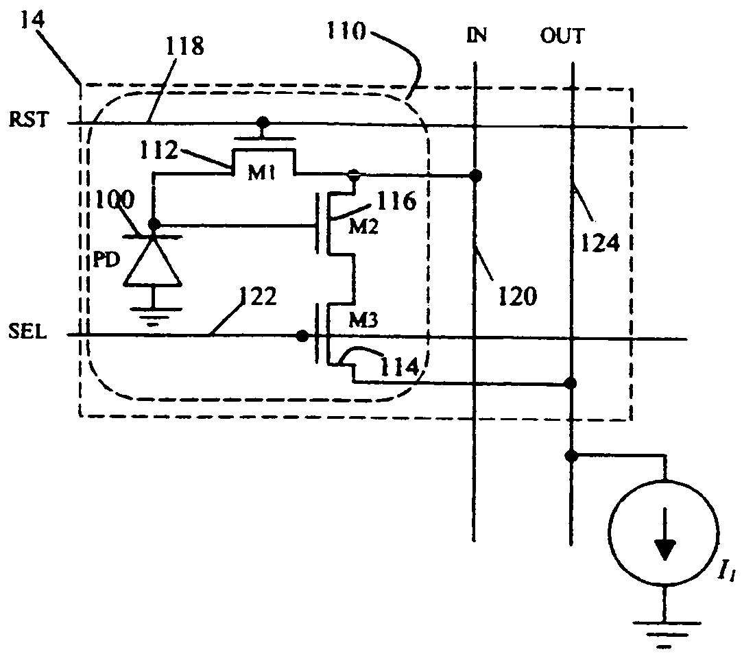
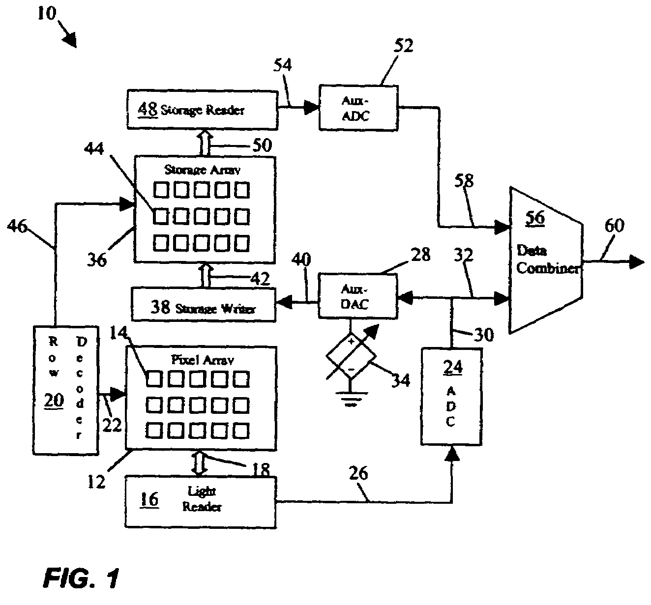
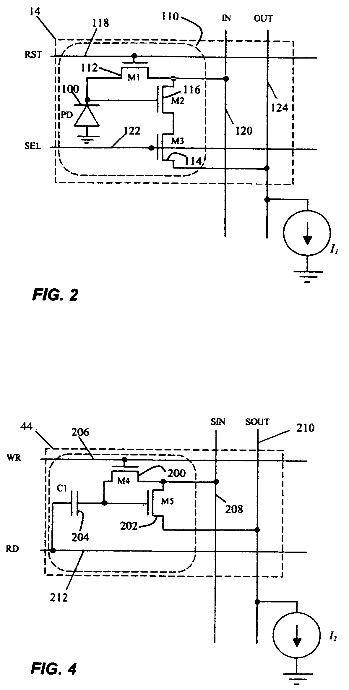
[0029]Disclosed is an image sensor that has one or more pixels within a pixel array. The pixel array may be coupled to a control circuit and one or more subtraction circuits. The control circuit may cause each pixel to provide a first reference output signal and a reset output signal. The control circuit may then cause each pixel to provide a light response output signal and a second reference output signal. The light response output signal corresponds to the image that is to be captured by the sensor.

[0030]The subtraction circuit may provide a difference between the reset output signal and the first reference output signal to create a noise signal that is stored in memory. The subtraction circuit may also provide a difference between the light response output signal and the second reference output signal to create a normalized light response output signal. The noise signal may then be subtracted from the normalized light response output signal to generate the output data of the sen...


PUM


Abstract

An image sensor that has one or more pixels within a pixel array. The pixel array may be coupled to a control circuit and one or more subtraction circuits. The control circuit may cause each pixel to provide a first reference output signal and a reset output signal. The control circuit may then cause each pixel to provide a light response output signal and a second reference output signal. The light response output signal corresponds to the image that is to be captured by the sensor. The subtraction circuit may provide a difference between the reset output signal and the first reference output signal to create a noise signal that is stored in memory. The subtraction circuit may also provide a difference between the second reference output signal and the light response output signal to create a normalized light response output signal. The noise signal may then be subtracted from the normalized light response output signal to generate the output data of the sensor. The second reference output signal is the same as the first reference output signal so that the process in essence subtracts the reset noise from the light response signal.

Description

CROSS REFERENCE TO RELATED APPLICATIONS[0001]This application is a continuation application claiming priority to U.S. patent application Ser. No. 10 / 183,218, filed Jun. 26, 2002, which now U.S. Pat. No. 6,795,117, claims priority under 35 U.S.C. §119(e) to provisional Application No. 60 / 333,216, filed on Nov. 6, 2001; provisional application No. 60 / 338,465, filed on Dec. 3, 2001 and provisional application No. 60 / 345,672 filed on Jan. 5, 2002.BACKGROUND OF THE INVENTION[0002]1. Field of the Invention[0003]The subject matter disclosed generally relates to the field of semiconductor image sensors.[0004]2. Background Information[0005]Photographic equipment such as digital cameras and digital camcorders contain electronic image sensors that capture light for processing into a still or video image, respectively. There are two primary types of electronic image sensors, charge coupled devices (CCDs) and complimentary metal oxide semiconductor (CMOS) sensors. CCD image sensors have relative...

Claims


Application Information

Patent Timeline
Patent Type & Authority Patents(United States)
IPC IPC(8): H04N5/335H01L27/146H04N1/32H04N1/40H04N5/363H04N5/374H04N5/378H04N9/04H04N9/64
CPCH04N1/32358H04N1/32475H04N1/32491H04N1/40H04N5/3575H04N5/363H01L27/14643H04N9/045H04N9/64G11C11/407H04N5/378H04N9/642H04N2201/0081H04N2201/3292H04N25/616H04N25/65H04N25/771H04N25/70H04N25/77H04N25/75
Inventor TAY, HIOK NAM
Owner CANDELA MICROSYST
Why Eureka
Try Eureka